SLUSBE4B January 2014 – June 2014
PRODUCTION DATA.
- 1 Features
- 2 Applications
- 3 Description
- 4 Simplified Diagram
- 5 Revision History
- 6 Pin Configuration and Functions
- 7 Specifications
-
8 Detailed Description
- 8.1 Overview
- 8.2 Functional Block Diagram
- 8.3
Feature Description
- 8.3.1 A6 Coil Specification
- 8.3.2 EMI Shield
- 8.3.3 I2C Interface
- 8.3.4 Active or Passive Wake-up State
- 8.3.5 Smart Key or Immobilizer Handling
- 8.3.6 Option Select Pins
- 8.3.7 LED Modes
- 8.3.8 Foreign Object Detection (FOD) and Parasitic Metal Object Detect (PMOD) CalibrationForeign Object Detection (FOD) and Parasitic Metal Object Detect (PMOD) Calibration description.
- 8.3.9 Shut Down via External Thermal Sensor or Trigger
- 8.3.10 Fault Handling and Indication
- 8.3.11 Power Transfer Start Signal
- 8.3.12 Power-On Reset
- 8.3.13 External Reset, RESET Pin
- 8.3.14 Trickle Charge and CS100
- 8.3.15 Over-Voltage Protection Over-Voltage Protection section.
- 8.4 Device Functional Modes
- 9 Applications and Implementation
- 10Power Supply Recommendations
- 11Layout
- 12Device and Documentation Support
- 13Mechanical, Packaging, and Orderable Information
Package Options
Mechanical Data (Package|Pins)
- RGZ|48
Thermal pad, mechanical data (Package|Pins)
- RGZ|48
Orderable Information
9 Applications and Implementation
9.1 Application Information
The bq500414Q device is a wireless power transmitter controller designed for automotive applications. It integrates all functions required to control wireless power transfer to a WPC v1.1 compliant receiver. There are several tools available for the design of the system. See the product folder on www.ti.com for more details. The following sections highlight some of the system design considerations.
9.2 Typical Application
The application block diagram for the transmitter is shown in Figure 9.
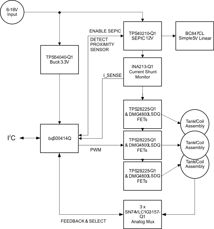 Figure 9. bq500414Q System Diagram
9.2.1 Design Requirements
9.2.1.1 Capacitor Selection
Capacitor selection is critical to proper system operation. The total capacitance value of 2 x 68-nF ( 2 x (68-nF + 5.6-nF) in the center coil) is required in the resonant tank. This is the WPC system compatibility requirement, not a guideline.
NOTE
A total capacitance value of 2 x 68-nF (additional 2 x 5.6-nF center coil) (C0G dielectric type, 100V rating) is required in the resonant tank to achieve the correct resonance frequency.
The capacitors chosen must be rated for at least 100 V and must be of a high quality C0G dielectric (sometimes also called NP0). These are typically available in a 5% tolerance, which is adequate. The use of X7R types or below is not recommended if WPC compliance is required because critical WPC Certification Testing, such as the minimum modulation or ensured power requirements, might fail.
The designer can combine capacitors to achieve the desired capacitance value. Various combinations can work depending on market availability. All capacitors must be of C0G types, not mixed with any other dielectric types.
9.2.1.2 Current Monitoring Requirements
The bq500414Q is WPC1.1 ready. In order to enable the PMOD or FOD features, current monitoring must be provided in the design.
For proper scaling of the current monitor signal, the current sense resistor should be 40-mΩ and the current shunt amplifier should have a gain of 50, such as the INA213Q1. For FOD accuracy, the current sense resistor must be a quality component with 1% tolerance, at least 1/4-Watt rating, and a temperature stability of ±200 PPM. Proper current sensing techniques in the application hardware should also be observed.
9.2.1.3 All Unused Pins
All unused pins can be left open unless otherwise indicated. Please refer to the Pin Functions table. Grounding of unused pins, if it is an option, can improve PCB layout.
9.2.1.4 Input Regulators
The bq500414Q requires 3.3-VDC to operate. A buck converter is used to step down from the automotive rail voltage, such as the TPS54040 used in this design.
The power train bridge circuitry requires 12 V, and it is fed from a SEPIC converter using the TPS40210 controller. Since the automotive rail voltage can vary widely, this acts as a type of pre-regulator.
9.2.1.5 Input Power Requirements
The design works with 6-V to 16-V input voltage. A6 Tx type requires 12-V system voltage. A SEPIC converter TPS40210 is included in the design to work with 6-V to 16-V input voltage for automotive application.
9.2.2 Detailed Design Procedure
To begin the design process a few parameters must be decided upon. The design needs to know the following:
- Active or Passive Wake-up State
- EMI Shield
- LED Mode
- Number of Tx coils (1, 2, or 3)
9.2.2.1 Active or Passive Wake-up State
bq500414Q detects the pin 18 ~EN_PWR voltage at power up. If it's high, the bq500414Q will not send any analog ping to detect the Rx, until SHUTDOWN command is disabled through I2C. A proximity sensor could be used with this feature.
9.2.2.2 EMI Shield
EMI shield can help improve EMI performance. Pin 21 EMI_SHIELD is used to indicate if EMI shield is in use.
9.2.2.3 LED mode
bq500414Q can directly drive three LED outputs (pin 7 LED_A, pin 8 LED_B, and pin 9 LED_C). Select one of the desired LED indication schemes by choosing the selection resistor connected between pin 44 LED_MODE and GND.
9.2.2.4 Number of Transmitter Coils
bq500414Q supports 1, 2, or 3 coils. Please refer to the product folder on www.ti.com for more information on the 3-coil design.
9.2.3 Application Performance Plots
The system efficiency with A6 Tx type coil is shown in Figure 10. The SEPIC converter that provides 12-V causes some efficiency drop.
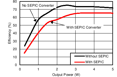 Figure 10. System Efficiency With A6 Tx Type Coil, With and Without SEPIC Converter
The frequency shift operation is shown in the Qi Sniffer capture in Figure 10. The Rx is placed on the Tx with no load. The operating frequency is 154-kHz. Then a FREQ_SHIFT command is issued through I2C, to shift the operating frequency to 190-kHz for 50,000-ms. After requested 50,000 ms, the operating frequency goes back to its previous operating frequency, which is 154-kHz.
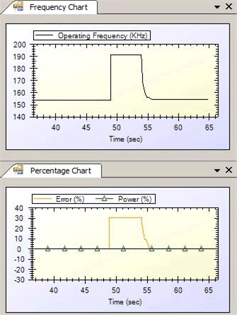 Figure 11. Qi Sniffer Capture of Frequency Shift Operation
bq500414Q EVM is tested per CISPR25 EMI specification with and without the EMI shield. The measurement results show > 24-dB improvement with the EMI shield at 5-W output power.
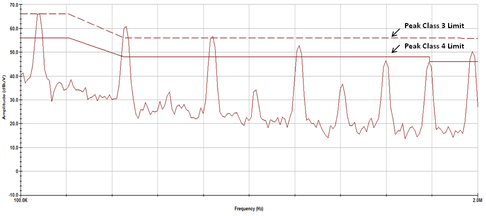 Figure 12. CISPR25 EMI Testing Result Without the EMI Shield at 5-W Output Power
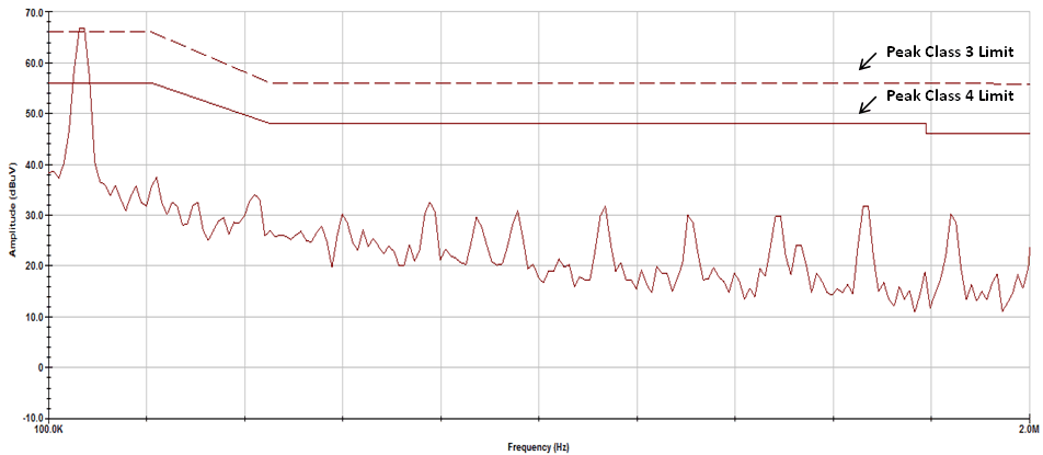 Figure 13. CISPR25 EMI Testing Result With the EMI Shield at 5-W Output Power