SLUSCD3A August 2015 – October 2015
PRODUCTION DATA.
- 1 Features
- 2 Applications
- 3 Description
- 4 Revision History
- 5 Pin Configuration and Functions
- 6 Specifications
-
7 Detailed Description
- 7.1 Overview
- 7.2 Functional Block Diagram
- 7.3
Feature Description
- 7.3.1 A11 Coil Specification
- 7.3.2 Option Select Pins
- 7.3.3 LED Modes
- 7.3.4 Foreign Object Detection (FOD) and FOD Calibration
- 7.3.5 Shut Down Through External Thermal Sensor or Trigger
- 7.3.6 Fault Handling and Indication
- 7.3.7 Power Transfer Start Signal
- 7.3.8 Power-On Reset
- 7.3.9 Trickle Charge and CS100
- 7.4 Device Functional Modes
- 8 Application and Implementation
- 9 Power Supply Recommendations
- 10Layout
- 11Device and Documentation Support
- 12Mechanical, Packaging, and Orderable Information
Package Options
Mechanical Data (Package|Pins)
- RHA|40
Thermal pad, mechanical data (Package|Pins)
- RHA|40
Orderable Information
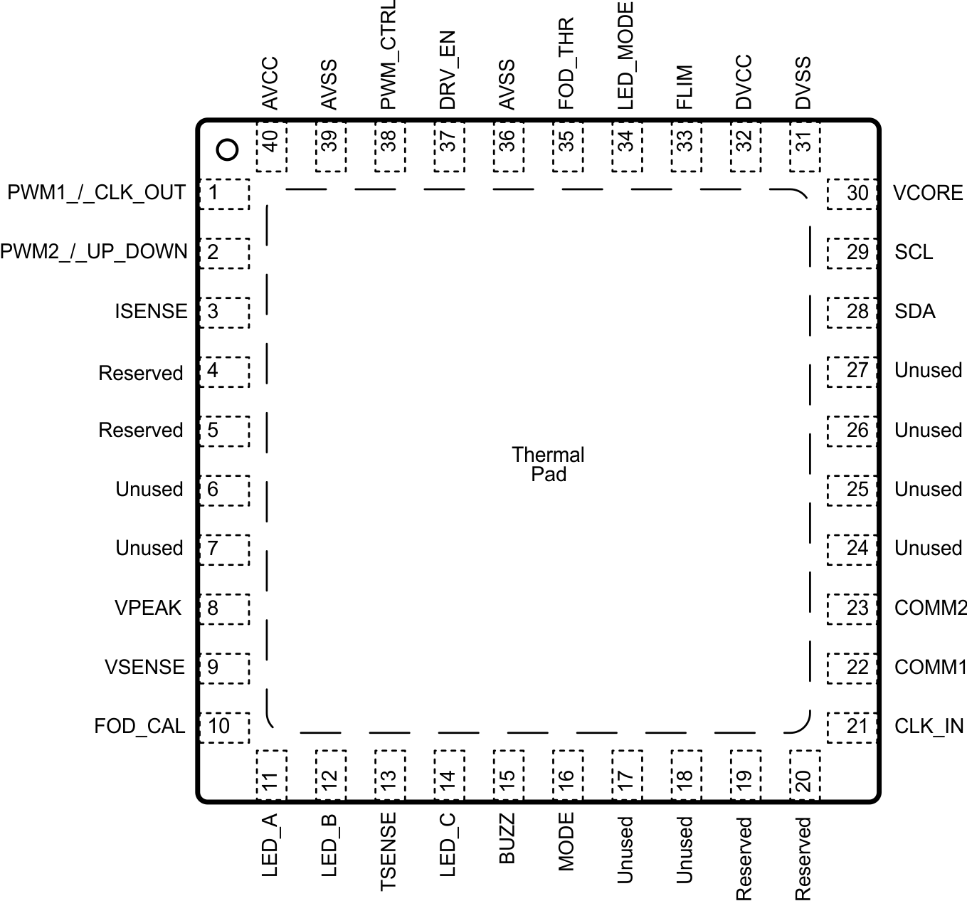
5 Pin Configuration and Functions
RHA Package
40-Pin VQFN
Top View

Pin Functions
| PIN | I/O | DESCRIPTION | |
|---|---|---|---|
| NAME | NO. | ||
| AVCC | 40 | — | Analog l power supply. |
| AVSS | 36, 39 | — | Analog ground. |
| BUZZ | 15 | O | DC buzzer output. A 400-ms DC pulse when charging begins. This could also be connected to an LED via 1-kΩ resistor. |
| CLK_IN | 21 | I | CLK_OUT signal from the internal oscillator of the bq50002 Analog Front End. |
| COMM1 | 22 | I | Communication channel 1. Typically generated by the bq50002 Analog Front End. |
| COMM2 | 23 | I | Communication channel 2. Typically generated by the bq50002 Analog Front End. |
| DRV_EN | 37 | O | Driver enable. |
| DVCC | 32 | — | Digital power supply. |
| DVSS | 31 | — | Digital ground. |
| FLIM | 33 | I | Leave floating to conform to the WPC specification 205-kHz maximum operating frequency. Pull down with a 10-kΩ resistor to limit the maximum frequency to 190 kHz. |
| FOD_CAL | 10 | I | FOD calibration. |
| FOD_THR | 35 | I | FOD threshold. |
| ISENSE | 3 | I | Input current sense. |
| LED_A | 11 | O | Connect to a LED via 1-kΩ resistor for status indication. Typically GREEN. |
| LED_B | 12 | O | Connect to a LED via 1-kΩ resistor for status indication. Typically RED. |
| LED_C | 14 | O | Connect to a LED via 1-kΩ resistor for status indication. Typically ORANGE. |
| LED_MODE | 34 | I | LED mode selection. |
| MODE | 16 | O | MODE is an output intended for use by the bq50002 Analog Front End indicating whether adjustments should be made using frequency (when MODE is low) or duty-cycle (when MODE is high). |
| PWM1 / CLK_OUT | 1 | O | If PWM_CTRL is high, this pin outputs PWM1 signal. If PWM_CTRL is low, this pin outputs clock signal. The rising edge of the clock is used to adjust frequency (MODE low) or duty cycle (MODE high) output of the bq50002 Analog Front End. |
| PWM_CTRL | 38 | O | PWM_CTRL is an output intended for use by the bq50002 Analog Front End to select whether its PWM outputs are generated internally within the bq50002 itself (PWM_CTRL HIGH), or whether they are simply passed through from external signals (PWM_CTRL LOW). |
| PWM2 / UP_DOWN | 2 | O | If PWM_CTRL is high, this pin outputs PWM2 signal. If PWM_CTRL is low, this pin is used to adjust the frequency (MODE low) or duty cycle (MODE high) of the external PWM output. If this signal is high, it decrease frequency or increase duty cycle. If this signal is low, it increases frequency or decreases duty cycle output of the bq50002 Analog Front End. |
| Reserved | 4 | I | Leave this pin open. |
| Reserved | 5 | I | Unused |
| Reserved | 19 | I | Reserved. Leave this pin open. |
| Reserved | 20 | I/O | Reserved. Leave this pin open. |
| SCL | 29 | I/O | 10-kΩ pull-up resistor to 3-V supply. I2C Clock. |
| SDA | 28 | I/O | 10-kΩ pull-up resistor to 3-V supply. I2C Data. |
| TSENSE | 13 | I | Temperature sensing for safety shutdown. Connect to 3 V via 10-kΩ resistor if unused. |
| Unused | 6 | I | Leave this pin open. |
| Unused | 7 | I/O | Leave this pin open. |
| Unused | 17, 18, 24–27 | I/O | Leave this pin open. |
| VCORE | 30 | — | Regulated internal core power supply. Connect via 0.4-µF capacitor to ground. |
| VPEAK | 8 | I | Peak coil voltage. |
| VSENSE | 9 | I | Input voltage sense. |