SLUSCN3A July 2016 – August 2016
PRODUCTION DATA.
- 1 Features
- 2 Applications
- 3 Description
- 4 Revision History
- 5 Pin Configuration and Functions
- 6 Specifications
-
7 Detailed Description
- 7.1 Overview
- 7.2 Functional Block Diagram
- 7.3
Feature Description
- 7.3.1 A11 Coil Specification
- 7.3.2 Option Select Pins
- 7.3.3 LED Modes
- 7.3.4 Foreign Object Detection (FOD) and FOD Calibration
- 7.3.5 Shut Down Through External Thermal Sensor or Trigger
- 7.3.6 Fault Handling and Indication
- 7.3.7 Power Transfer Start Signal
- 7.3.8 Power-On Reset
- 7.3.9 Trickle Charge and CS100
- 7.4 Device Functional Modes
- 8 Application and Implementation
- 9 Power Supply Recommendations
- 10Layout
- 11Device and Documentation Support
- 12Mechanical, Packaging, and Orderable Information
Package Options
Mechanical Data (Package|Pins)
- RHA|40
Thermal pad, mechanical data (Package|Pins)
- RHA|40
Orderable Information
8 Application and Implementation
NOTE
Information in the following applications sections is not part of the TI component specification, and TI does not warrant its accuracy or completeness. TI’s customers are responsible for determining suitability of components for their purposes. Customers should validate and test their design implementation to confirm system functionality.
8.1 Application Information
The bq500511A device is a wireless power transmitter controller designed for 5W WPC compliant applications when paired with the bq50002A. The pair integrates all functions required to control wireless power transfer to a WPC v1.2 compliant receiver. Several tools are available for the design of the system. See the product folder on www.ti.com for more details. The following sections highlight some of the system design considerations.
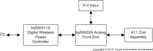 Figure 7. bq500511A System Block Diagram
The I2C port is accessed by the FOD tuning tool and can provide a level of system monitoring and evaluation.
The SDA and SCL lines of the I2C bus must be pulled up (as shown in the Figure 8) if the I2C port is utilized. They may be left floating if no I2C function is required. The logic reference generated by the bq50002A Analog Front End is 3 V, so care should be taken to ensure that if the Master I2C device also has pull-up resistors to a higher reference, that the the 3-V reference to the bq500511A is not affected. Specifically, only one set of pull-up resistors should be populated, either on the I2C Master bus or on the bq500511A system board, but not both.
Additional details on I2C use and capabilities can be obtained by contacting TI.
8.2 Typical Application
The bq500511A controller, when paired with bq50002A integrated Analog Front End device, requires a minimum of external components to implement a WPC 1.2 Wireless Power Transmitter system.
As shown in the application schematic, external components are used to implement the following functions:
- Resonant tank circuit
- Demodulator input signal conditioning
- Human interface (LED and Buzzer)
- Current sensing
- Voltage sensing
- Temperature sensing
- System Configuration: Foreign Objection Detection (FOD) threshold and calibration, LED mode
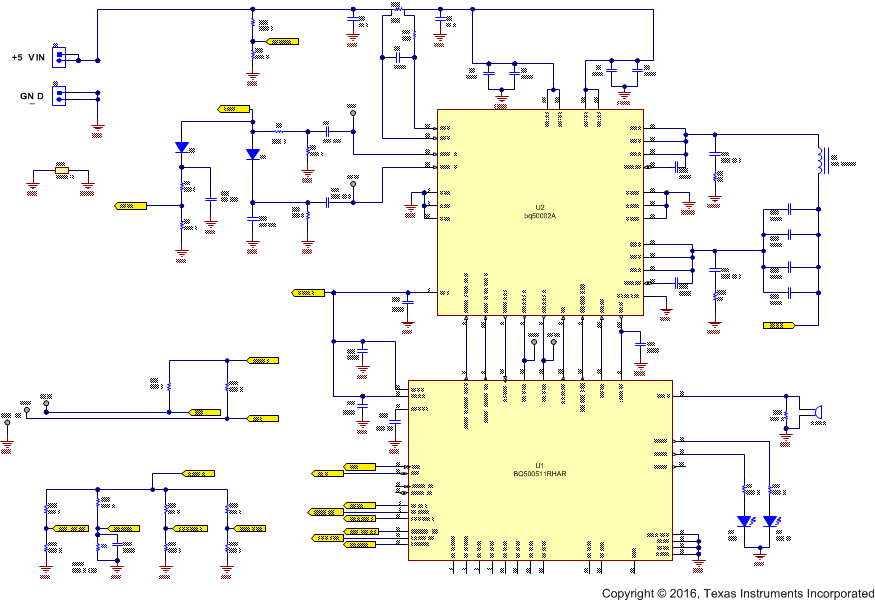 Figure 8. bq500511A Application Schematic
8.2.1 Design Requirements
For this design example, use the parameter listed in Table 3 as the input parameter.
Table 3. Design Parameters
| DESIGN PARAMETER | VALUE |
|---|---|
| WPC coil type | A11 |
8.2.2 Detailed Design Procedure
8.2.2.1 Capacitor Selection
Capacitor selection is critical to proper system operation. The total capacitance value of 4 × 100 nF is required in the resonant tank. This is the WPC system compatibility requirement, not a guideline.
NOTE
A total capacitance value of 4 × 100 nF (C0G dielectric type, 50-V rating) is required in the resonant tank to achieve the correct resonance frequency. The capacitors chosen must be rated for at least 50 V and must be of a high-quality C0G dielectric (sometimes also called NP0). These are typically available in a 5% tolerance, which is adequate. TI does not recommend the use of X7R types or below if WPC compliance is required because critical WPC Certification Testing, such as the minimum modulation or guaranteed power test, might fail. The designer can combine capacitors to achieve the desired capacitance value. Various combinations can work depending on market availability. All capacitors must be of C0G types (not mixed with any other dielectric types).
8.2.2.2 Current Monitoring Requirements
The bq500511A is WPC v1.2 ready. To enable the FOD feature, current monitoring is provided in the bq50002A Analog Front End. For proper scaling of the current monitor signal, the current sense resistor should be 20 mΩ. For FOD accuracy, the current sense resistor must be a quality component with 0.5% tolerance, at least 1/4-W rating, and a temperature stability of ±200 PPM.
8.2.2.3 Input Voltage Monitoring
The VSENSE input is used to calculate power for the FOD function, and to detect the supply drooping when the bq500511A is receiving power from an insufficient adapter (for example from a weak USB port). The VSENSE input should reflect the input source voltage and should be scaled with a resistor divider comprising a 76.8 kΩ over 10 kΩ.
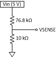 Figure 9. VSENSE Signal Conditioning
8.2.2.4 Tank Voltage Monitoring
The VPEAK input is used to estimate losses in the power components for the FOD function. The VPEAK input should reflect the envelope of the tank voltage (i.e. the node directly between the resonant capacitors and the primary coil) and should be buffered with a diode (100 V, 0.2 A) and scaled with a resistor divider comprising a 113 kΩ over 7.5 kΩ, with a 2200-pF filter capacitor.
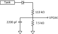 Figure 10. VPEAK Signal Conditioning
8.2.2.5 All Unused Pins
All unused pins can be left open unless otherwise indicated. Refer to the table in the Pin Configuration and Functions section. To improve PCB layout, ground unused pins, if it is an option.
8.2.2.6 Input Regulation
The bq500511A requires 3 VDC to operate. The regulator in the bq50002A provides this voltage rail eliminating the need for any external regulation.
8.2.2.7 System Input Power Requirements
The design works with 5-V input voltage to the bq50002A. The WPC defined A11 TX type requires 5-V system voltage in order to deliver 5 W of output power from the receiver.
8.2.2.8 LED Modes
The bq500511A can directly drive three LED outputs (pin 11 (LED-A), pin 12 (LED-B), and pin 14 (LED-C)). Select one of the desired LED indication schemes through the voltage on LED_MODE (pin 34) by choosing appropriate values for the resistor divider.
8.2.3 Application Curves
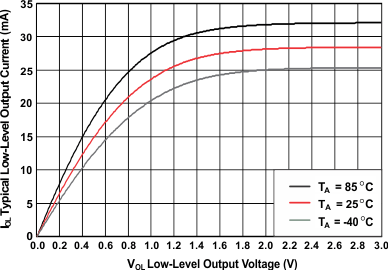
| VCC = 3 V |
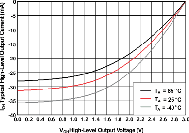
| VCC = 3 V |