SLUSAD3C June 2011 – October 2016
PRODUCTION DATA.
- 1 Features
- 2 Applications
- 3 Description
- 4 Revision History
- 5 Pin Configuration and Functions
- 6 Specifications
-
7 Detailed Description
- 7.1 Overview
- 7.2 Functional Block Diagram
- 7.3
Feature Description
- 7.3.1
Analog-to-Digital Conversion (ADC)
- 7.3.1.1 General Features
- 7.3.1.2 3-to-6 Series Cell Configuration
- 7.3.1.3 Cell Voltage Measurements
- 7.3.1.4 GPAI or VBAT Measurements
- 7.3.1.5 Temperature Measurement
- 7.3.1.6 ADC Band-Gap Voltage Reference
- 7.3.1.7 Conversion Control
- 7.3.1.8 Secondary Protection
- 7.3.1.9 Cell Overvoltage Fault Detection (COV)
- 7.3.1.10 Cell Undervoltage Fault Detection (CUV)
- 7.3.1.11 Overtemperature Detection
- 7.3.1.12 Fault and Alert Behavior
- 7.3.1.13 Secondary Protector Built-In Self-Test Features
- 7.3.2 Cell Balancing
- 7.3.3 Other Features and Functions
- 7.3.4 Communications
- 7.3.5 Device-to-Device Vertical Bus (VBUS) Interface
- 7.3.6 Packet Formats
- 7.3.7 Device Addressing
- 7.3.8 Changes and Enhancements for bq76PL536A
- 7.3.1
Analog-to-Digital Conversion (ADC)
- 7.4 Device Functional Modes
- 7.5 Programming
- 7.6
Register Maps
- 7.6.1 I/O Register Details
- 7.6.2 Register Types
- 7.6.3 Register Details
- 7.6.4 GPAI (0x01, 0x02) Register
- 7.6.5 VCELLn Register (0x03…0x0e)
- 7.6.6 TEMPERATURE1 Register (0x0f, 0x10)
- 7.6.7 TEMPERATURE2 Register (0x11, 0x12)
- 7.6.8 ALERT_STATUS Register (0x20)
- 7.6.9 FAULT_STATUS Register (0x21)
- 7.6.10 COV_FAULT Register (0x22)
- 7.6.11 CUV_FAULT Register (0x23)
- 7.6.12 PARITY_H Register (0x24) (PRESULT_A (R/O))
- 7.6.13 PARITY_H Register (0x25) (PRESULT_B (R/O))
- 7.6.14 ADC_CONTROL Register (0x30)
- 7.6.15 IO_CONTROL Register (0x31)
- 7.6.16 CB_CTRL Register (0x32)
- 7.6.17 CB_TIME Register (0x33)
- 7.6.18 ADC_CONVERT Register (0x34)
- 7.6.19 SHDW_CTRL Register (0x3a)
- 7.6.20 ADDRESS_CONTROL Register (0x3b)
- 7.6.21 RESET Register (0x3c)
- 7.6.22 TEST_SELECT Register (0x3d)
- 7.6.23 E_EN Register (0x3f)
- 7.6.24 FUNCTION_CONFIG Register (0x40)
- 7.6.25 IO_CONFIG Register (0x41)
- 7.6.26 CONFIG_COV Register (0x42)
- 7.6.27 CONFIG_COVT Register (0x43)
- 7.6.28 CONFIG_UV Register (0x44)
- 7.6.29 CONFIG_CUVT Register (0x45)
- 7.6.30 CONFIG_OT Register (0x46)
- 7.6.31 CONFIG_OTT Register (0x47)
- 7.6.32 USERx Register (0x48-0x4b) (USER1-4)
- 8 Application and Implementation
- 9 Power Supply Recommendations
- 10Layout
- 11Device and Documentation Support
- 12Mechanical, Packaging, and Orderable Information
Package Options
Mechanical Data (Package|Pins)
- PAP|64
Thermal pad, mechanical data (Package|Pins)
- PAP|64
Orderable Information
8 Application and Implementation
NOTE
Information in the following applications sections is not part of the TI component specification, and TI does not warrant its accuracy or completeness. TI’s customers are responsible for determining suitability of components for their purposes. Customers should validate and test their design implementation to confirm system functionality.
8.1 Application Information
The bq76PL536A is a series-cell Lithium-Ion battery monitor and secondary protector for Uninterruptible Power Systems (UPS), E-Bikes and Scooters, Large-Format Battery Systems, and so forth. To allow for optimal performance in the end application, special consideration must be taken to ensure minimization of measurement error through proper printed circuit board (PCB) layout.
8.1.1 Anti-Aliasing Filter
An anti-aliasing filter is required for each VCn input VC6–VC1, consisting of a 1-kΩ, 1% series resistor and 100-nF capacitor. Good-quality components should be used. A 1% resistor is recommended, because the resistor creates a small error by forming a voltage divider with the input impedance of the part. The part is factory-trimmed to compensate for the error introduced by the filter.
8.1.2 Host SPI Interface Pin States
The CS_H pin is active-low. The host asserts the pin to a logic zero to initiate communications. The CS pin should remain low until the end of the current packet. When the CS_H pin is asserted, the SPI receiver and interface of the device are reset and resynchronized. This action ensures that a slave device that has lost synchronization during a previous transmission or as the result of noise on the bus does not remain permanently hung. CS_H must be driven false (high) between packets; see Timing Characteristics – AC SPI Data Interface for timing details.
8.2 Typical Application
Figure 57 shows the recommended reference design components.
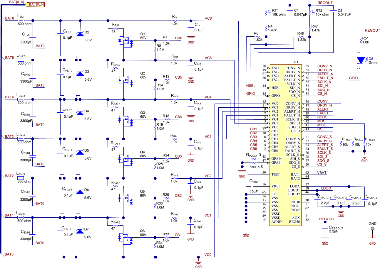 Figure 57. Application Schematic
8.2.1 Design Requirements
For this design example, use the parameters listed in Table 26.
Table 26. Design Parameters
| PARAMETER | DESCRIPTION | EXAMPLE VALUE | UNIT |
|---|---|---|---|
| CEMI | EMI Capacitor | 3300 | pF |
| CFILT | Filter Capacitor | 0.1 | µF |
| CIN | Input Capacitor | 0.1 | µF |
| CREGOUT | REGOUT Capacitor | 2.2 (minimum) | µF |
| CVDDA_1 | Internal analog 5-V LDO bypass connection 1 | 2.2 | µF |
| CVDDA_2 | Internal analog 5-V LDO bypass connection 2 | 0.2 | µF |
| CVDD_D_1 | Capacitor for internal digital 5-V LDO bypass connection 1 | 2.2 | µF |
| CVDD_D_2 | Capacitor for internal digital 5-V LDO bypass connection 2 | 0.2 | µF |
| CVREF | VREF Capacitor | 10 | µF |
| LEMI | EMI Ferrite Resistor | 500 | Ω |
| RBAL | Balance Resistor | 47 | Ω |
| RIN | Input Resistor | 1 | kΩ |
| RPULL1-RPULL3 | Pullup Resistors for digital open-drain I/O | 10 | kΩ |
| RPULL4-RPULL5 | Pullup Resistors for general-purpose (differential) analog input (GPAI), connect to VSS if unused | kΩ |
8.2.2 Detailed Design Procedure
Use the following for the procedure for the recommended front-end circuit:
- Select the RC filter closest to the cell for filter requirements. Additional poles can be added with a differential capacitor to get very low fc.
- ADC is calibrated to use RIN = 1 kΩ and CIN = 0.1 µF.
- Select Zener diode for lowest possible reverse leakage.
- A balance FET gate-protection diode is required (available internally).
- Select the capacitors for LDO Filters according to Table 26.
- LDO1 and LDO2 require a 2.2-µF ceramic capacitor for stability. These pins are tied together internally. Tie LDO1 to LDOD2 externally.
- For pullup supply, the following information applies:
- REG50 turns off in SLEEP mode
- Use LDOD for pullups in normal use
- Use REG50 for programming EEPROM (LDOD will see 7 V)
- Connect GPAI+ and GPA– to VSS if unused
- Select low impedance and polarized connectors. Numbered or colored connectors are also good options.
- Select the input Zener TVS so that it clamps below 5.6 Vdc, with low-leakage current, and must be able to handle transient surge energy
- Select capacitors based on temperature and environment with voltages well above the operating voltage
- Select balancing MOSFETs according to the following:
- Low turn on threshold voltage (must turn on with the lowest cell voltage)
- Drain-to-source voltage and gate-to-source voltage
- Power dissipation
- Current based on selected bleed resistor value
- Select the Bleed Resistor according to the following:
- Value based on desired current
- Wattage to handle the current and temperature rise such as 4.2 V × 47 = 0.089 A ∴ 0.37 W)
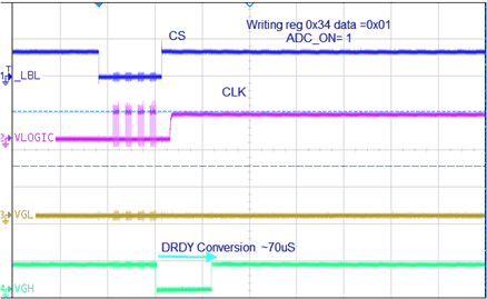
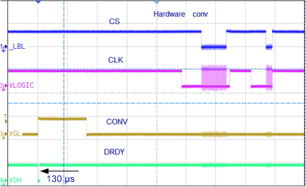
8.2.3 Application Curves
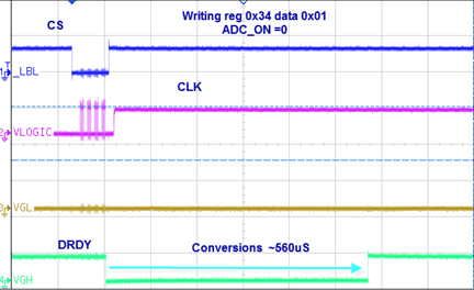
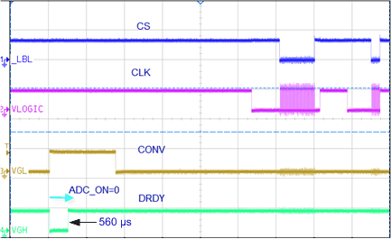
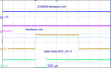
8.3 Other Schematics
The device generic part number, bq76PL536, is shown in these schematics.
Full-size reference schematics are available from TI on request.
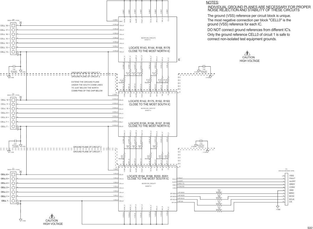 Figure 63. Schematic (Page 1 of 4)
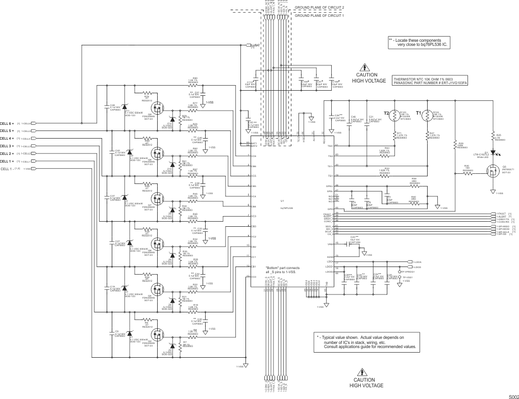 Figure 64. Schematic (Page 2 of 4)
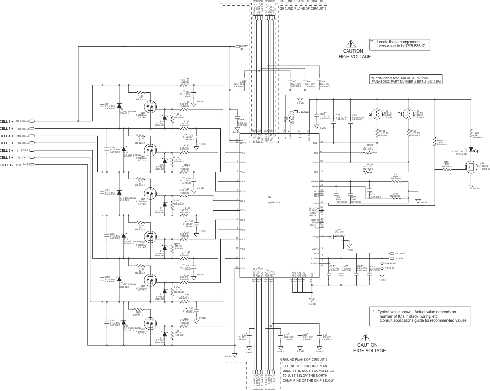 Figure 65. Schematic (Page 3 of 4)
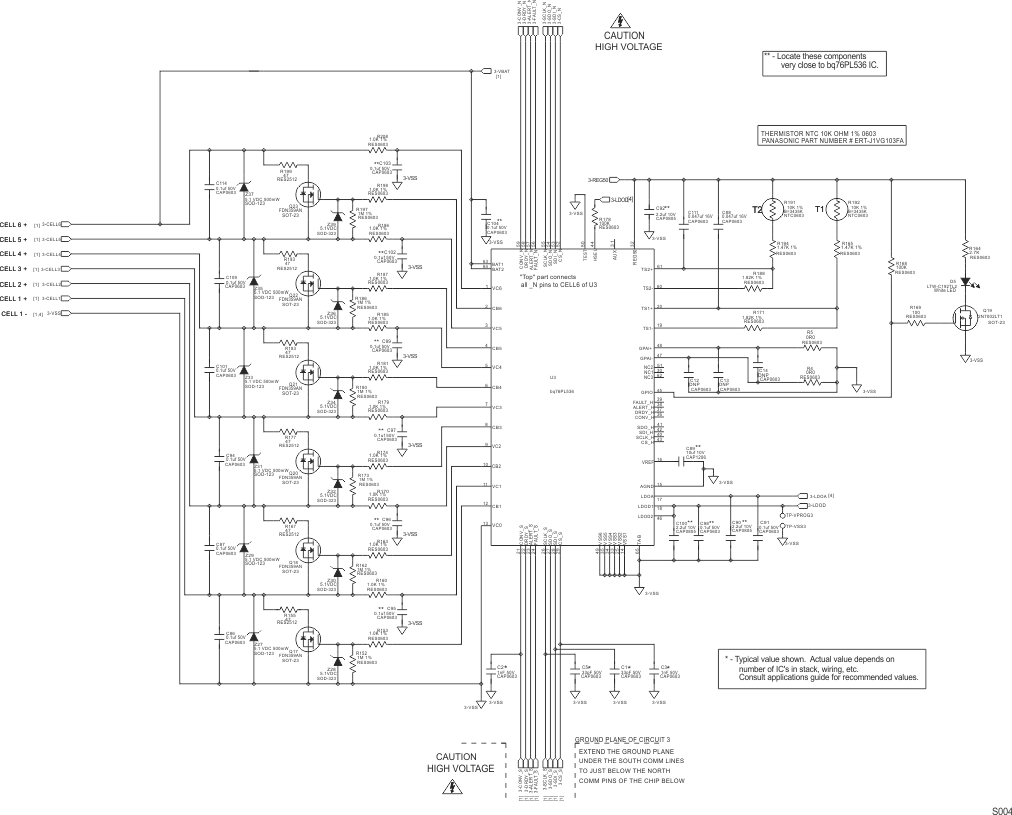 Figure 66. Schematic (Page 4 of 4)
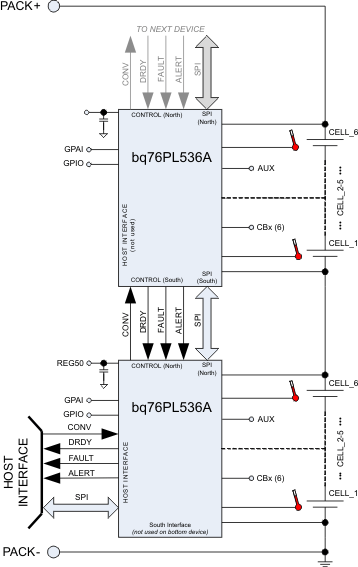 Figure 67. Simplified System Connection