SLUSB48 July 2014
PRODUCTION DATA.
- 1 Features
- 2 Applications
- 3 Description
- 4 Simplified Schematic
- 5 Revision History
- 6 Description (continued)
- 7 Pin Configuration and Functions
-
8 Specifications
- 8.1 Absolute Maximum Ratings
- 8.2 Handling Ratings
- 8.3 Recommended Operating Conditions
- 8.4 Thermal Information
- 8.5 Electrical Characteristics: Supply Current
- 8.6 Electrical Characteristics: I/O
- 8.7 Electrical Characteristics: ADC
- 8.8 Electrical Characteristics: Power-On Reset
- 8.9 Electrical Characteristics: Oscillator
- 8.10 Electrical Characteristics: Data Flash Memory
- 8.11 Electrical Characteristics: Register Backup
- 8.12 SMBus Timing Specifications
- 8.13 Typical Characteristics
- 9 Detailed Description
- 10Application and Implementation
- 11Power Supply Recommendations
- 12Layout
- 13Device and Documentation Support
- 14Mechanical, Packaging, and Orderable Information
Package Options
Mechanical Data (Package|Pins)
- DBT|30
Thermal pad, mechanical data (Package|Pins)
Orderable Information
12 Layout
12.1 Layout Guidelines
12.1.1 Power Supply Decoupling Capacitor
Power supply decoupling from VCC to ground is important for optimal operation of the bq78350. To keep the loop area small, place this capacitor next to the IC and use the shortest possible traces. A large-loop area renders the capacitor useless and forms a small-loop antenna for noise pickup.
Ideally, the traces on each side of the capacitor must be the same length and run in the same direction to avoid differential noise during ESD. If possible, place a via near the VSS pin to a ground plane layer.
Placement of the RBI capacitor is not as critical. It can be placed further away from the IC.
12.1.2 MRST Connection
The MRST pin controls the gas gauge reset state. The connections to this pin must be as short as possible in order to avoid any incoming noise. Direct connection to VCC is possible if the reset functionality is not desired or necessary.
If unwanted resets are found, one or more of the following solutions may be effective:
- Add a 0.1-μF capacitor between MRST and ground.
- Provide a 1-kΩ pull up resistor to VCC at MRST.
- Surround the entire circuit with a ground pattern.
If a test point is added at MRST, it must be provided with a 10-kΩ series resistor.
12.1.3 Communication Line Protection Components
The 5.6-V Zener diodes, which protect the bq78350 communication pins from ESD, must be located as close as possible to the pack connector. The grounded end of these Zener diodes must be returned to the PACK(–) node, rather than to the low-current digital ground system. This way, ESD is diverted away from the sensitive electronics as much as possible.
12.1.4 ESD Spark Gap
Protect the SMBus clock, data, and other communication lines from ESD with a spark gap at the connector. The following pattern is recommended, with 0.2-mm spacing between the points.
 Figure 16. Recommended Spark-Gap Pattern Helps Protect Communication Lines From ESD
12.2 Layout Example
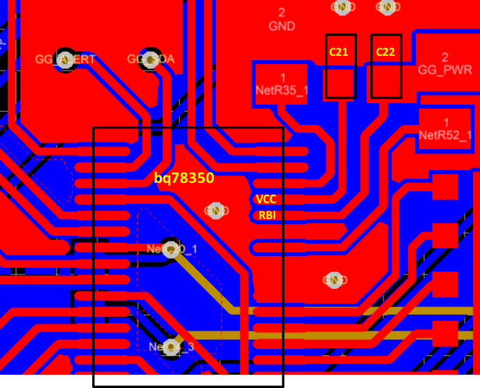 Figure 17. bq78350 Layout