SCHS097F November 1998 – March 2017 CD40106B
PRODUCTION DATA.
- 1 Features
- 2 Applications
- 3 Description
- 4 Revision History
- 5 Pin Configuration and Functions
- 6 Specifications
- 7 Parameter Measurement Information
- 8 Detailed Description
- 9 Application and Implementation
- 10Power Supply Recommendations
- 11Layout
- 12Device and Documentation Support
- 13Mechanical, Packaging, and Orderable Information
Package Options
Mechanical Data (Package|Pins)
Thermal pad, mechanical data (Package|Pins)
Orderable Information
8 Detailed Description
8.1 Overview
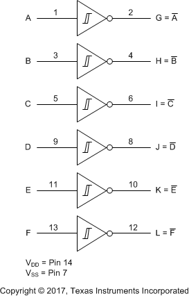
The CD40106B device contains six independent inverters with schmitt trigger inputs.. They perform the Boolean function Y = A in positive logic.
Schmitt-Trigger inputs are designed to provide a minimum separation between positive and negative switching thresholds. This allows for noisy or slow inputs that would cause problems such as oscillation or excessive current consumption.
8.2 Functional Block Diagram

8.3 Feature Description
The CD40106B has standardized symmetrical output characteristics and a wide operating voltage from 3 V to
18 V with quiescent current of 20 µA tested at 20 V. These devices have transition times of tTLH = tTHL = 50 ns (typical) at 10 V. The operating temperature is from –55°C to +125°C. Schmitt trigger inputs on this device support slow or noisy input signals.
8.4 Device Functional Modes
Table 1 lists the functional modes of the CD40106B.
Table 1. Function Table
| INPUT | OUTPUT |
|---|---|
| H | L |
| L | H |