SCHS287C December 2023 – May 2024 CD54AC240 , CD54AC244 , CD54ACT240 , CD54ACT241 , CD54ACT244 , CD74AC240 , CD74AC244 , CD74ACT240 , CD74ACT241 , CD74ACT244
PRODUCTION DATA
- 1
- 1 Features
- 2 Description
- 3 Pin Configuration and Functions
- 4 Specifications
- 5 Parameter Measurement Information
- 6 Detailed Description
- 7 Application and Implementation
- 8 Device and Documentation Support
- 9 Revision History
- 10Mechanical, Packaging, and Orderable Information
Package Options
Refer to the PDF data sheet for device specific package drawings
Mechanical Data (Package|Pins)
- N|20
- DW|20
Thermal pad, mechanical data (Package|Pins)
Orderable Information
3 Pin Configuration and Functions
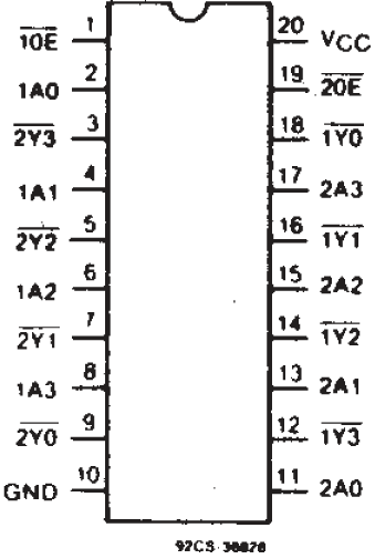
 Figure 3-1 CD54/74AC, ACT240 Types Terminal
Assignment
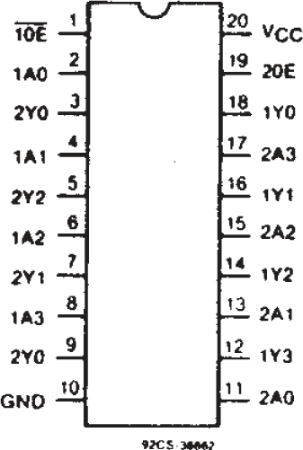
 Figure 3-3 CD54/74AC, ACT244 Types Terminal
Assignment
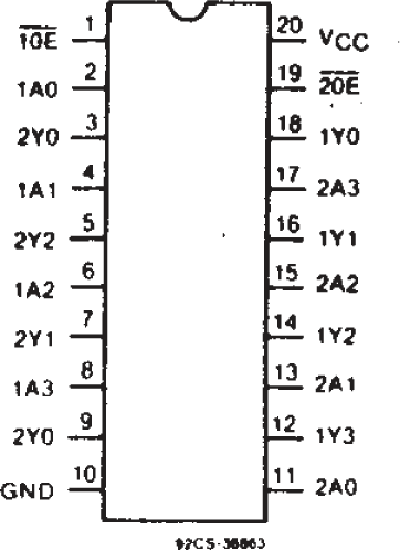
 Figure 3-2 CD54/74AC, ACT241 Types Terminal
Assignment
Figure 3-2 CD54/74AC, ACT241 Types Terminal
AssignmentTable 3-1 Pin Functions
| PIN | TYPE(1) | DESCRIPTION | |
|---|---|---|---|
| NO. | NAME | ||
| 1OE | 1 | I | Bank 1, output enable, active low |
| 1A0 | 2 | I | Bank 1, channel 1 input |
| 2Y3 | 3 | O | Bank 2, channel 4 output |
| 1A1 | 4 | I | Bank 1, channel 2 input |
| 2Y2 | 5 | O | Bank 2, channel 3 output |
| 1A2 | 6 | I | Bank 1, channel 3 input |
| 2Y1 | 7 | O | Bank 2, channel 2 output |
| 1A3 | 8 | I | Bank 1, channel 4 input |
| 2Y0 | 9 | O | Bank 2, channel 1 output |
| GND | 10 |
G |
Ground |
| 2A0 | 11 | I | Bank 2, channel 1 input |
| 1Y3 | 12 | O | Bank 1, channel 4 output |
| 2A1 | 13 | I | Bank 2, channel 2 input |
| 1Y2 | 14 | O | Bank 1, channel 3 output |
| 2A2 | 15 | I | Bank 2, channel 3 input |
| 1Y1 | 16 | O | Bank 1, channel 2 output |
| 2A3 | 17 | I | Bank 2, channel 4 input |
| 1Y0 | 18 | O | Bank 1, channel 1 output |
| 2OE | 19 | I | Bank 2, output enable, active low |
| VCC | 20 |
P |
Positive supply |
| Thermal pad(2) | — | The thermal pad can be connected to GND or left floating. Do not connect to any other signal or supply | |
(1) I = input, O = output, I/O = input or
output, G = ground, P = power.
(2) RKS package only.