SCAS918D June   2013  – February 2024 CDCE913-Q1 , CDCEL913-Q1

PRODUCTION DATA  

  1.   1
  2. Features
  3. Applications
  4. Description
  5. Device Comparison
  6. Pin Configuration and Functions
  7. Specifications
    1. 6.1 Absolute Maximum Ratings
    2. 6.2 ESD Ratings
    3. 6.3 Recommended Operating Conditions
    4. 6.4 Thermal Information
    5. 6.5 Electrical Characteristics
    6. 6.6 Timing Requirements
    7. 6.7 Typical Characteristics
  8. Parameter Measurement Information
  9. Detailed Description
    1. 8.1 Overview
    2. 8.2 Functional Block Diagram
    3. 8.3 Feature Description
      1. 8.3.1 Control Terminal Configuration
      2. 8.3.2 Default Device Configuration
      3. 8.3.3 I2C Serial Interface
      4. 8.3.4 Data Protocol
    4. 8.4 Device Functional Modes
      1. 8.4.1 SDA and SCL Hardware Interface
    5. 8.5 Programming
  10. Application and Implementation
    1. 9.1 Application Information
    2. 9.2 Typical Application
      1. 9.2.1 Design Requirements
      2. 9.2.2 Detailed Design Procedure
        1. 9.2.2.1 Spread-Spectrum Clock (SSC)
        2. 9.2.2.2 PLL Frequency Planning
        3. 9.2.2.3 Crystal Oscillator Start-Up
        4. 9.2.2.4 Frequency Adjustment With Crystal Oscillator Pulling
        5. 9.2.2.5 Unused Inputs and Outputs
        6. 9.2.2.6 Switching Between XO and VCXO Mode
      3. 9.2.3 Application Curves
    3. 9.3 Power Supply Recommendations
    4. 9.4 Layout
      1. 9.4.1 Layout Guidelines
      2. 9.4.2 Layout Example
  11. 10Register Maps
    1. 10.1 I2C Configuration Registers
  12. 11Device and Documentation Support
    1. 11.1 Documentation Support
      1. 11.1.1 Related Documentation
    2. 11.2 Receiving Notification of Documentation Updates
    3. 11.3 Support Resources
    4. 11.4 Trademarks
    5. 11.5 Electrostatic Discharge Caution
    6. 11.6 Glossary
  13. 12Revision History
  14. 13Mechanical, Packaging, and Orderable Information

Package Options

Mechanical Data (Package|Pins)
Thermal pad, mechanical data (Package|Pins)
Orderable Information

Spread-Spectrum Clock (SSC)

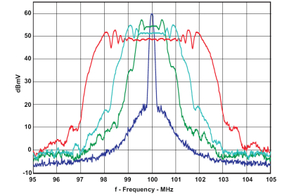
Spread-spectrum modulation is a method to spread emitted energy over a larger bandwidth. In clocking, spread spectrum can reduce electromagnetic interference (EMI) by reducing the level of emission from the clock distribution network.
GUID-52B55944-EBC9-4EB8-901D-4BC628D53E77-low.gif
CDCS502 with a 25-MHz crystal, FS = 1, fOUT = 100 MHz, and 0%, ±0.5, ±1%, and ±2% SSC
Figure 9-4 Comparison Between Typical Clock Power Spectrum and Spread-Spectrum Clock

Spread-spectrum clocking can be used to help reduce EMI to meet design specifications. For example, a specified EMI threshold of 55 dB/mV would require ±1% spread-spectrum clocking to meet this requirement.