SCAS844G August 2007 – January 2024 CDCE949 , CDCEL949
PRODUCTION DATA
- 1
- 1 Features
- 2 Applications
- 3 Description
- 4 Pin Configuration and Functions
- 5 Specifications
- 6 Parameter Measurement Information
- 7 Detailed Description
- 8 Application and Implementation
- 9 Register Maps
- 10Device and Documentation Support
- 11Revision History
- 12Mechanical, Packaging, and Orderable Information
Package Options
Mechanical Data (Package|Pins)
- PW|24
Thermal pad, mechanical data (Package|Pins)
Orderable Information
8.2.2.2 PLL Frequency Planning
At a given input frequency (ƒIN), use Equation 1 to calculate the output frequency (ƒOUT) of the CDCEx949.
Equation 1. 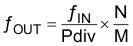
where
- M (1 to 511) and N (1 to 4095) are the multiplier/divide values of the PLL
- Pdiv (1 to 127) is the output divider
Use Equation 2 to calculate the target VCO frequency (ƒVCO) of each PLL.
Equation 2. 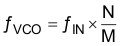
The PLL internally operates as fractional divider and requires the following multiplier/divider settings:
- N
- P = 4 – int(log2N/M; if P < 0 then P = 0
- Q = int(N'/M)
- R = N′ – M × Q
where
N′ = N × 2P
N ≥ M;
80 MHz ≤ ƒVCO ≤ 230 MHz
16 ≤ Q ≤ 63
0 ≤ P ≤ 4
0 ≤ R ≤ 51
| Example: | |||
| for ƒIN = 27 MHz; M = 1; N = 4; Pdiv = 2 | for ƒIN = 27 MHz; M = 2; N = 11; Pdiv = 2 | ||
| → | fOUT = 54 MHz | → | fOUT = 74.25 MHz |
| → | fVCO = 108 MHz | → | fVCO = 148.50 MHz |
| → | P = 4 – int(log24) = 4 – 2 = 2 | → | P = 4 – int(log25.5) = 4 – 2 = 2 |
| → | N' = 4 × 22 = 16 | → | N' = 11 × 22 = 44 |
| → | Q = int(16) = 16 | → | Q = int(22) = 22 |
| → | R = 16 – 16 = 0 | → | R = 44 – 44 = 0 |
The values for P, Q, R, and N’ are automatically calculated when using TI Pro-Clock™ software.