SLPS551B May 2015 – February 2022 CSD25484F4
PRODUCTION DATA
- 1Features
- 2Applications
- 3Description
- 4Revision History
- 5Specifications
- 6Device and Documentation Support
- 7Mechanical, Packaging, and Orderable Information
Package Options
Mechanical Data (Package|Pins)
- YJJ|3
Thermal pad, mechanical data (Package|Pins)
Orderable Information
3 Description
This 80-mΩ, –20-V, P-Channel FemtoFET™ MOSFET is designed and optimized to minimize the footprint in many handheld and mobile applications. This technology is capable of replacing standard small signal MOSFETs while providing at least a 60% reduction in footprint size.
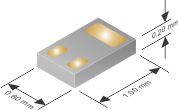
 Figure 3-1 Typical Package Dimensions
Product Summary
| TA = 25°C | TYPICAL VALUE | UNIT | ||
|---|---|---|---|---|
| VDS | Drain-to-source voltage | –20 | V | |
| Qg | Gate charge total (–4.5 V) | 1090 | pC | |
| Qgd | Gate charge gate-to-drain | 150 | pC | |
| RDS(on) | Drain-to-source
on-resistance | VGS = –1.8 V | 405 | mΩ |
| VGS = –2.5 V | 150 | |||
| VGS = –4.5 V | 93 | |||
| VGS = –8.0 V | 80 | |||
| VGS(th) | Threshold voltage | –0.95 | V | |
Device
Information
| DEVICE | QTY | MEDIA | PACKAGE(1) | SHIP |
|---|---|---|---|---|
| CSD25484F4 | 3000 | 7-Inch Reel | Femto (0402) 1.00-mm × 0.60-mm Land Grid Array (LGA) | Tape and Reel |
| CSD25484F4T | 250 |
(1) For all available packages, see the orderable addendum at the end of the data sheet.
Absolute Maximum Ratings
| TA = 25°C | VALUE | UNIT | |
|---|---|---|---|
| VDS | Drain-to-source voltage | –20 | V |
| VGS | Gate-to-source voltage | –12 | V |
| ID | Continuous drain current(1) | –2.5 | A |
| IDM | Pulsed drain current(1)(2) | –22 | A |
| IG | Continuous gate clamp current | –35 | mA |
| Pulsed gate clamp current(2) | –350 | ||
| PD | Power dissipation(1) | 500 | mW |
| V(ESD) | Human-body model (HBM) | 4 | kV |
| Charged-device model (CDM) | 2 | ||
| TJ, Tstg | Operating junction, storage temperature | –55 to 150 | °C |
(1) Typical RθJA = 85°C/W on 1-in2 (6.45-cm2), 2-oz
(0.071-mm) thick Cu pad on a 0.06-in (1.52-mm) thick FR4 PCB.
(0.071-mm) thick Cu pad on a 0.06-in (1.52-mm) thick FR4 PCB.
(2) Pulse duration ≤ 100 μs, duty cycle ≤ 1%.
Figure 3-2 Top View