SLPS384D March   2013  – April 2015 CSD87588N

PRODUCTION DATA.  

  1. 1Features
  2. 2Applications
  3. 3Description
  4. 4Revision History
  5. 5Specifications
    1. 5.1 Absolute Maximum Ratings
    2. 5.2 Recommended Operating Conditions
    3. 5.3 Thermal Information
    4. 5.4 Power Block Performance
    5. 5.5 Electrical Characteristics
    6. 5.6 Typical Power Block Device Characteristics
    7. 5.7 Typical Power Block MOSFET Characteristics
  6. 6Application and Implementation
    1. 6.1 Application Information
      1. 6.1.1 Power Loss Curves
      2. 6.1.2 Safe Operating Curves (SOA)
      3. 6.1.3 Normalized Curves
      4. 6.1.4 Calculating Power Loss and SOA
        1. 6.1.4.1 Design Example
        2. 6.1.4.2 Calculating Power Loss
        3. 6.1.4.3 Calculating SOA Adjustments
  7. 7Layout
    1. 7.1 Layout Guidelines
      1. 7.1.1 Electrical Performance
      2. 7.1.2 Thermal Performance
    2. 7.2 Layout Example
  8. 8Device and Documentation Support
    1. 8.1 Trademarks
    2. 8.2 Electrostatic Discharge Caution
    3. 8.3 Glossary
  9. 9Mechanical, Packaging, and Orderable Information
    1. 9.1 CSD87588N Package Dimensions
    2. 9.2 Land Pattern Recommendation
    3. 9.3 Stencil Recommendation (100 µm)
    4. 9.4 Stencil Recommendation (125 µm)
    5. 9.5 Pin Drawing
    6. 9.6 CSD87588N Embossed Carrier Tape Dimensions

Package Options

Mechanical Data (Package|Pins)
  • MPA|5
Thermal pad, mechanical data (Package|Pins)
Orderable Information

1 Features

  • Half-Bridge Power Block
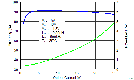
  • 90% System Efficiency at 20 A
  • Up to 25 A Operation
  • High Density – 5 mm x 2.5 mm LGA Footprint
  • Double Side Cooling Capability
  • Ultra-Low Profile – 0.48 mm Max
  • Optimized for 5 V Gate Drive
  • Low Switching Losses
  • Low Inductance Package
  • RoHS Compliant
  • Halogen Free
  • Pb Free

2 Applications

  • Synchronous Buck Converters
    • High-Current, Low Duty Cycle Applications
  • Multiphase Synchronous Buck Converters
  • POL DC-DC Converters

3 Description

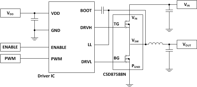
The CSD87588N NexFET™ power block II is a highly-optimized design for synchronous buck applications offering high current and high efficiency capability in a small 5 mm × 2.5 mm outline. Optimized for 5 V gate drive applications, this product offers an efficient and flexible solution capable of providing a high density power supply when paired with any 5 V gate driver from an external controller/driver.


Ordering Information(1)

Device Media Qty Package Ship
CSD87588N 13-Inch Reel 2500 5 x 2.5 LGA Tape and Reel
CSD87588NT 7-Inch Reel 250
  1. For all available packages, see the orderable addendum at the end of the data sheet.
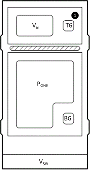

CSD87588N Pin_Out.gif

Typical Circuit

CSD87588N Front_Page_Img_3.gif

Typical Power Block Efficiency and Power Loss
CSD87588N front_page_SLPS384_F.png