SLPS416C June   2014  – March 2015 CSD95372AQ5M

PRODUCTION DATA.  

  1. Features
  2. Applications
  3. Description
  4. Revision History
  5. Pin Configuration and Functions
  6. Specifications
    1. 6.1 Absolute Maximum Ratings
    2. 6.2 ESD Ratings
    3. 6.3 Recommended Operating Conditions
    4. 6.4 Thermal Information
    5. 6.5 Electrical Characteristics
    6. 6.6 Typical Power Stage Characteristics
  7. Detailed Description
    1. 7.1 Functional Block Diagram
    2. 7.2 Functional Description
      1. 7.2.1 Powering the CSD95372AQ5M and Gate Drivers
      2. 7.2.2 Undervoltage Lockout (UVLO) Protection
      3. 7.2.3 ENABLE
      4. 7.2.4 Power Up Sequencing
      5. 7.2.5 PWM
      6. 7.2.6 FCCM
      7. 7.2.7 TAO/FAULT (Thermal Analog Output/Protection Flag)
      8. 7.2.8 Over Temperature
      9. 7.2.9 Gate Drivers
  8. Application and Implementation
    1. 8.1 Application Information
    2. 8.2 Power Loss Curves
    3. 8.3 Safe Operating Curves (SOA)
    4. 8.4 Normalized Curves
    5. 8.5 Calculating Power Loss and SOA
      1. 8.5.1 Design Example
      2. 8.5.2 Calculating Power Loss
      3. 8.5.3 Calculating SOA Adjustments
  9. Layout
    1. 9.1 Layout Guidelines
      1. 9.1.1 Recommended Schematic Overview
      2. 9.1.2 Recommended PCB Design Overview
        1. 9.1.2.1 Electrical Performance
        2. 9.1.2.2 Thermal Performance
      3. 9.1.3 Sensing Performance
    2. 9.2 Layout Example
  10. 10Application Schematic
  11. 11Device and Documentation Support
    1. 11.1 Trademarks
    2. 11.2 Electrostatic Discharge Caution
    3. 11.3 Glossary
  12. 12Mechanical, Packaging, and Orderable Information
    1. 12.1 Mechanical Drawing
    2. 12.2 Recommended PCB Land Pattern
    3. 12.3 Recommended Stencil Opening

Package Options

Refer to the PDF data sheet for device specific package drawings

Mechanical Data (Package|Pins)
  • DQP|12
Thermal pad, mechanical data (Package|Pins)
Orderable Information

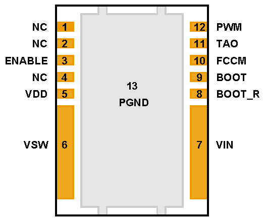
5 Pin Configuration and Functions

CSD95372AQ5M CSD95372A_pinout.png

Pin Functions

PIN DESCRIPTION
NAME NO.
NC 1, 2, 4 No connect, must leave floating.
ENABLE 3 Enables device operation. If ENABLE = logic HIGH, turns on device. If ENABLE = logic LOW, the device is turned off and both MOSFET gates are actively pulled low. An internal 100 kΩ pull down resistor will pull the ENABLE pin LOW if left floating.
VDD 5 Supply Voltage to Gate Driver and internal circuitry.
VSW 6 Phase node connecting the HS MOSFET Source and LS MOSFET Drain - pin connection to the output inductor.
VIN 7 Input Voltage Pin. Connect input capacitors close to this pin.
BOOT_R 8 Return path for HS gate driver, connected to VSW internally.
BOOT 9 Bootstrap capacitor connection. Connect a minimum of 0.1 µF 16 V X7R, ceramic capacitor from BOOT to BOOT_R pins. The bootstrap capacitor provides the charge to turn on the Control FET. The bootstrap diode is integrated.
FCCM 10 This pin enables the Diode Emulation function. When this pin is held LOW, Diode Emulation Mode is enabled for Sync FET. When FCCM is HIGH, the device operated in Forced Continuous Conduction Mode. An internal 5µA current source will pull the FCCM pin to VDD if left floating.
TAO/
FAULT
11 Temperature amplifier output. Reports a voltage proportional to the die temperature. An ORing diode is integrated in the IC. When used in multiphase application, a single wire can be used to connect the TAO pins of all the IC's. Only the highest temperature will be reported. TAO will be pulled up to 3.3 V if Thermal Shutdown occurs. TAO should be bypassed to PGND with a 1nF 16V X7R ceramic capacitor.
PWM 12 Pulse-width modulated Tri-state input from external controller. Logic LOW sets Control FET gate low and Sync FET gate high. Logic HIGH sets Control FET gate high and Sync FET gate low. Open or High Z sets both MOSFET gates low if greater than the Tri-State Shutdown Hold-off Time (t3HT).
PGND 13 Power ground.