SNAS515G July 2011 – December 2014 DAC161P997
PRODUCTION DATA.
- 1 Features
- 2 Application
- 3 Description
- 4 Revision History
- 5 Pin Configuration and Functions
- 6 Specifications
- 7 Detailed Description
- 8 Application and Implementation
- 9 Power Supply Recommendations
- 10Layout
- 11Device and Documentation Support
- 12Mechanical, Packaging, and Orderable Information
Package Options
Mechanical Data (Package|Pins)
- RGH|16
Thermal pad, mechanical data (Package|Pins)
- RGH|16
Orderable Information
8 Application and Implementation
NOTE
Information in the following applications sections is not part of the TI component specification, and TI does not warrant its accuracy or completeness. TI’s customers are responsible for determining suitability of components for their purposes. Customers should validate and test their design implementation to confirm system functionality.
8.1 Application Information
8.1.1 16-BIT DAC and Loop Drive
8.1.1.1 DC Characteristics
The DAC converts the 16-bit input code in the DACCODE register to an equivalent current output. The ∑Δ DAC output is a current pulse which is then filtered by a 3rd order RC low-pass filter and boosted to produce the loop current ILOOP at the device OUT pin.
Figure 21 shows the principle of operation of the DAC161P997 in the Loop Powered Transmitter - the circuit details were omitted for clarity. In this figure ID and IA represent supply (quiescent) currents of the internal digital and analog blocks. IAUX represents supply (quiescent) current of companion devices present in the system, such as the voltage regulator and the SWIF channel.
By observing that the control loop formed by the amplifier and the bipolar transistor forces the voltage across R1 and R2 to be equal, it can be shown that, under normal conditions, the ILOOP is dependent only on IDAC through the following relationship:

While ILOOP has a number of component currents, ILOOP = IDAC+ID+IA+IAUX+IE, it is only IE that is regulated by the loop to maintain the relationship shown above.
Since it is only IE’s magnitude that is controlled, not its direction, there is a lower limit to ILOOP. This limit is dependent on the fixed components IA and ID, and on system implementation through IAUX.
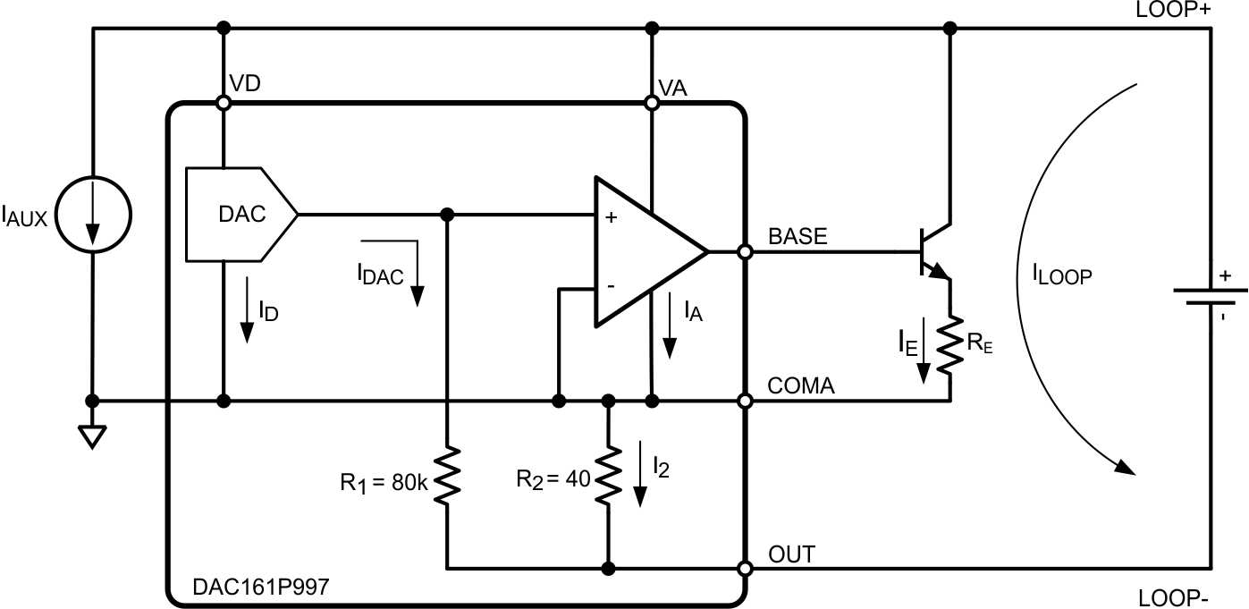 Figure 21. Loop-Powered Transmitter
Figure 22 shows the variant of the transmitter where the supply currents to the system blocks are provided by the local supply, and not the 4 - 20 mA loop Self-Powered Transmitter. Same basic relationship between the ILOOP and IDAC holds, but the component currents of ILOOP are only IDAC and IE.
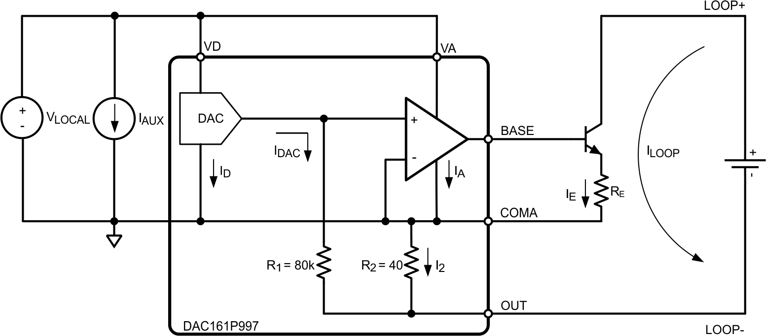 Figure 22. Self-Powered Transmitter
8.1.1.1.1 DC Input-Output Transfer Function
The output current sourced by the OUT pin of the device is expressed by:
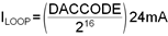
The valid DACCODE range is the full 16-bit code space (0x0000 to 0xFFFF), which results in the IDAC range of 0 to approximately 12 μA. This, however, does not result in the ILOOP range of 0 to 24 mA.
The maximum output current sourced out of OUT pin, ILOOP, is 24 mA. The minimum output current is dependent on the system implementation. The minimum output current is the sum of supply currents of the DAC161P997 internal blocks, IA, ID, and companion devices present in the system, IAUX. The last component current IE can theoretically be controlled down to 0 but, due to the stability considerations of the control loop, it is advised not to allow the IE to drop below 200 μA.
The graph in Figure 23 shows the DC transfer characteristic of the 4 - 20 mA transmitter, including minimum current limits. The minimum current limit for the Loop-Powered Transmitter is typically around 400 μA (ID+IA+IAUX+IE). The minimum current limit for the Self-Powered Transmitter is typically around 200 μA (IE).
Typical values for ID and IA are listed in Electrical Characteristics. IE depends on the BJT device used.
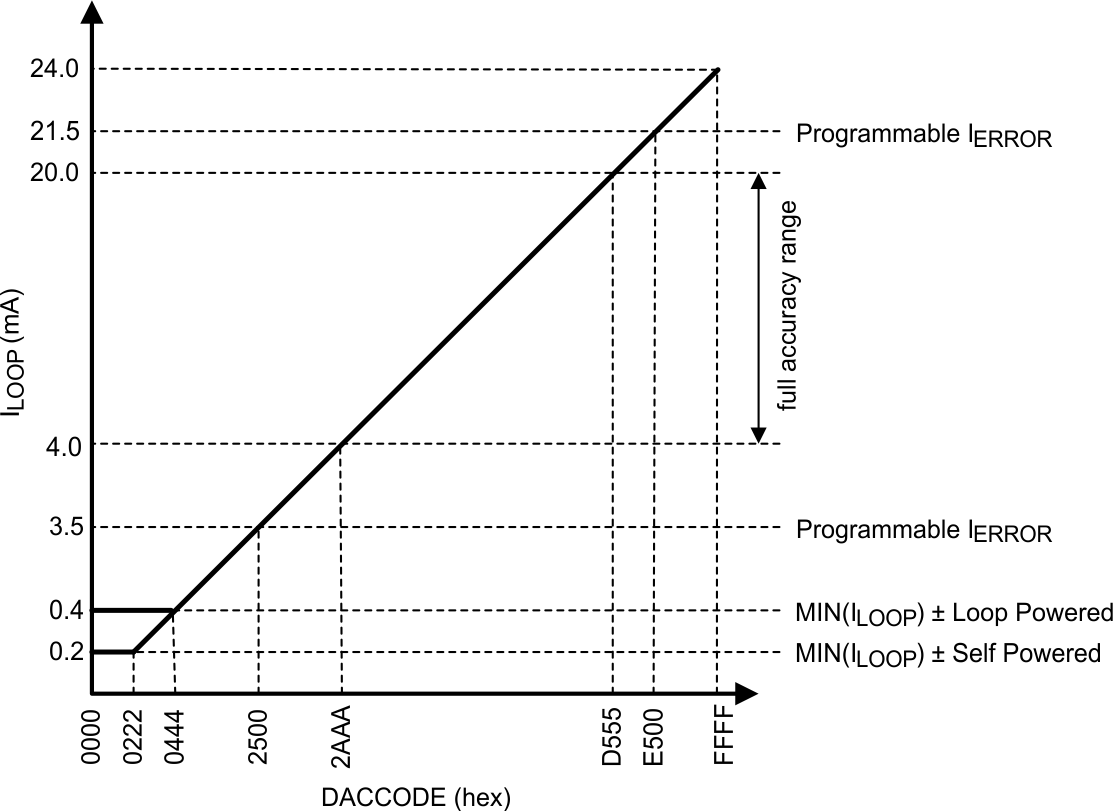 Figure 23. DAC-DC Transfer Function
8.1.1.1.2 Loop Interface
The DAC161P997 cannot directly interface to the typical 4 - 20 mA loop due to the excessive loop supply voltage. The loop interface has to provide the means of stepping down the LOOP Supply down to 3.6V. This can be accomplished with either a linear regulator (LDO) or switching regulator while keeping in mind that the regulator’s quiescent current will have direct effect on the minimum achievable ILOOP (see DC Input-Output Transfer Function).
The second component of the loop interface is the external NPN transistor (BJT). This device is part of the control circuit that regulates the transmitter’s output current (ILOOP). Since the BJT operates over the wide current range, spanning at least 4 - 20 mA, it is necessary to degenerate the emitter in order to stabilize transistor’s transconductance (gm). The degeneration resistor of 22Ω is suggested in typical applications. For circuit details, see Typical Application.
The NPN BJT should not be replaced with an N-channel FET (Field Effect Transistor) for the following reasons: discrete FET’s typically have high threshold voltages (VT), in the order of 1.5 V to 2 V, which is beyond the BASE output maximum range; discrete FET’s present higher load capacitance which may degrade system stability margins; and BASE output relies on the BJT’s base current for biasing.
8.1.1.1.3 Loop Compliance
The maximum V(LOOP+,LOOP-) potential is limited by the choice of step-down regulator, and the external BJT’s Collector Emitter breakdown voltage. For minimum V(LOOP+, LOOP−) potential consider Figure 22. Here, observe that V(LOOP+,LOOP−) ≅ min(VCE) + ILOOPRE + ILOOPR2 = min(VCE) + 0.53V + 0.96V = 3.66V, at ILOOP = 24mA. The voltage drop across internal R2 is specified in Electrical Characteristics.
8.1.1.2 AC Characteristics
The approximate frequency dependent characteristics of the loop drive circuit can be analyzed using the circuit in Figure 24:
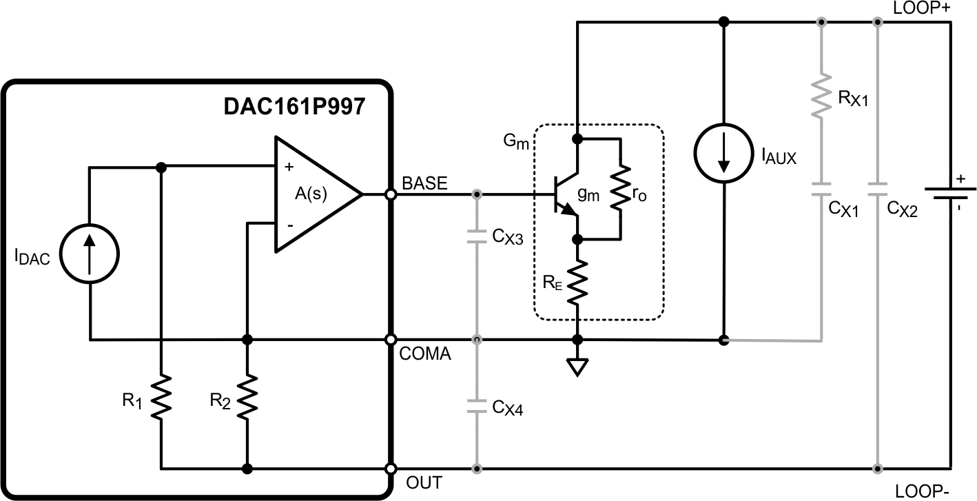 Figure 24. Capacitances Affecting Control Loop
Here it is assumed that the internal amplifier dominates the frequency response of the system, and it has a single pole response. The BJT’s response, in the bandwidth of the control loop, is assumed to be frequency independent and is characterized by the transconductance gm and the output resistance ro.
As in previous sections IDAC and IAUX represent the filtered output of the ∑Δ modulator and the quiescent current of the companion devices.
The circuit in Figure 24 can be further simplified by omitting the on-board capacitances, whose effect will be discussed in Stability, and by combining the amplifier, the external transistor and resistor RE into one Gm block. The resulting circuit is shown in Figure 25.
By assuming that the BJT’s output resistance (ro) is large, the loop current ILOOP can be expressed as:

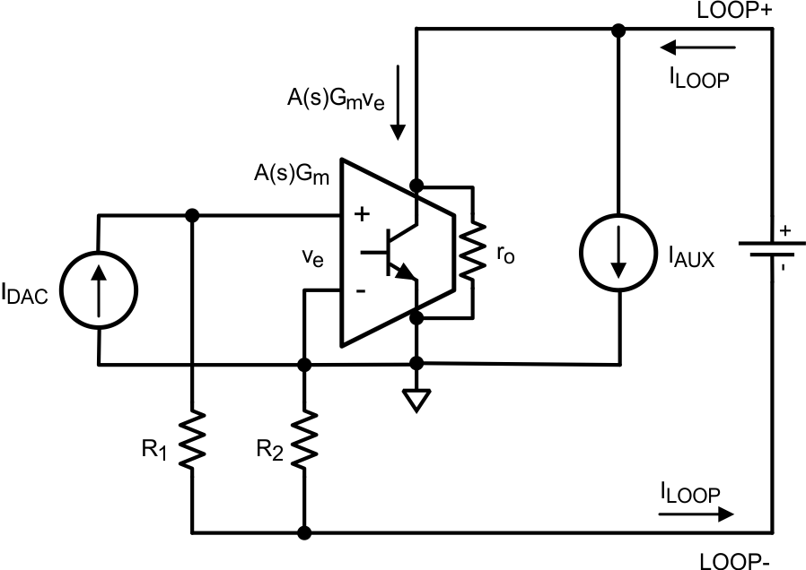 Figure 25. AC Analysis Model of a Transmitter
The sum of voltage drops around the path containing R1, R2 and ve is:

an assumption is made on the response of the internal amplifier::

By combining the above the final expression for the ILOOP as a function of 2 inputs IDAC and IAUX is:
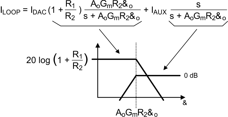
The result above reveals that there are 2 distinct paths from the inputs IDAC and IAUX to the output ILOOP. IDAC follows the low-pass, and the IAUX follows the high-pass path.
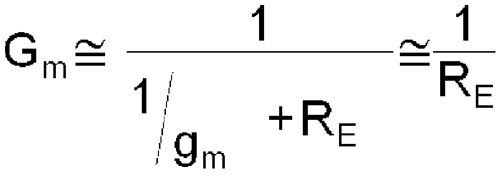
In both cases the corner frequency is dependent on the effective transconductance, Gm, of the external transistor. This implies that control loop dynamics could vary with the output current ILOOP if Gm were allowed to be just native device transconductance gm. This undesirable behavior is mitigated by the degenerating resistor RE which stabilizes Gm as follows:
This results in the frequency response which is largely independent of the output current ILOOP:
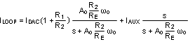
While the bandwidth of the IDAC path may not be of great consequence given the low frequency nature of the 4-20 mA current loop systems, the location of the pole in the IAUX path directly affects PSRR of the transmitter circuit. This is further discussed in PSRR.
8.1.1.2.1 Step Response
The transient input-output characteristics of the DAC161P997 are dominated by the response of the RC filter at the output of the ∑Δ DAC. Settling times due to step input are shown in Typical Characteristics.
8.1.1.2.2 Output Impedance
The output impedance is described as:

By considering the circuit in Figure 25, and setting IDAC = IAUX = 0, the following expression can be obtained:
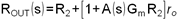
As in AC Characteristics an assumption can be made on the frequency response of the internal amplifier, and the effective transconductance Gm should be stabilized with external RE leading to:
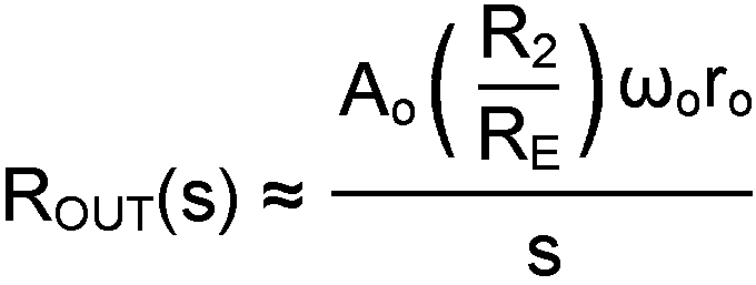
The output impedance of the transmitter is a product of the external BJT's output resistance ro, and the frequency characteristics of the internal amplifier. At low frequencies this results in a large impedance that does not significantly affect the output current accuracy.
8.1.1.2.3 PSRR
Power Supply Rejection Ratio is defined as the ability of the current control loop to reject the variations in the supply current of the companion devices, IAUX. Specifically:

It was shown in AC Characteristics that the IAUX affects ILOOP via the high-pass path whose corner frequency is dependent on the effective Gm of the external BJT. If that dependence were not mitigated with the degenerating resistor RE, the PSRR would be degraded at low output current ILOOP.
The typical PSRR performance of the transmitter shown in Typical Application is shown in Typical Characteristics.
8.1.1.2.4 Stability
The current control loop's stability is affected by the impedances present in the system. Figure 24 shows the simplified diagram of the control loop, formed by the on-board amplifier and an external BJT, and the lumped capacitances CX1 through CX4 that model any other external elements.
CX1 typically represents a local step-down regulator, or LDO, and any other companion devices powered from the LOOP+. This capacitance reduces the stability margins of the control loop, and therefore it should be limited. RX1 can be used to isolate CX1 from LOOP+ node and thus remedy the stability margin reduction. If RX1 = 0, CX1 cannot exceed 10 nF. RX1 = 200Ω is recommended if it can be tolerated. Minimum RX1 = 40Ω if CX1 exceeds 10 nF.
CX3 also adversely affects stability of the loop and it must be limited to 20 pF. CX4 affects the control loop in the same way as CX1, and it should be treated in the same way as CX1. CX2 is the only capacitance that improves stability margins of the control loop. Its maximum size is limited only by the safety requirements.
Stability is a function of ILOOP as well. Since ILOOP is approximately equal to the collector current of the external BJT, Gm of the BJT, and thus loop dynamics, depend on ILOOP. This dependence can be reduced by degenerating the emitter of the BJT with a small resistance as discussed in Loop Interface. Inductance in series with the LOOP+ and LOOP− do not significantly affect the control loop.
8.1.1.2.5 Noise and Ripple
The output of the DAC is a current pulse train. The transition density varies throughout the DAC input code range (ILOOP range). At the extremes of the code range, the transition density is the lowest which results in low frequency components of the DAC output passing through the RC filter. Hence, the magnitude of the ripple present in ILOOP is the highest at the ends of the transfer characteristic of the device (see Typical Characteristics).
It should be noted that at wide noise measurement bandwidth, it is the ripple due to the ∑Δ modulator that dominates the noise performance of the device throughout the entire code range of the DAC. This results in the “U” shaped noise characteristic as a function of output current. At narrow bandwidths, and particularly at mid-scale output currents, it is the amplifier driving the external BJT that starts to dominate as a noise source.
8.1.1.2.6 Digital Feedthrough
Digital feedthrough is indiscernible from the ripple induced by the ∑Δ modulator.
8.1.1.2.7 HART Signal Injection
The HART specification requires minimum suppression of the sensor signal in the HART signal band (1-2 kHz) of about 60 dB. The filter in Figure 26 below meets that requirement.
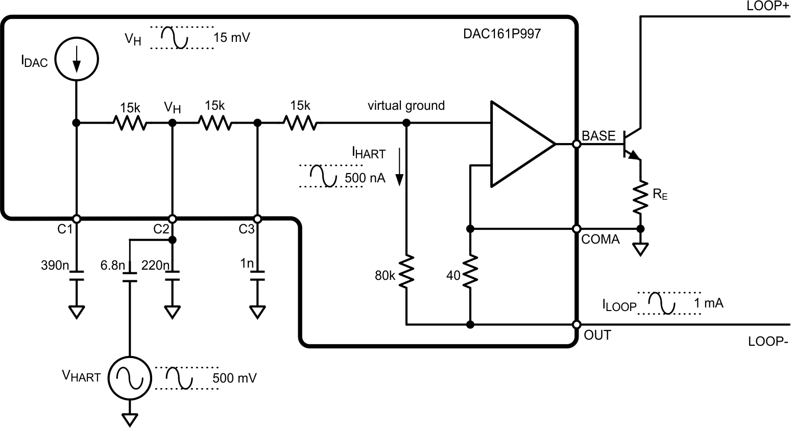 Figure 26. HART Signal Injection
8.1.1.2.8 RC Filter Limitation
In an effort to speed up the transient response of the device the user can reduce the capacitances associated with the low-pass filter at the output of the ∑Δ modulator. However, to maintain stability margins of the current control loop it is necessary to have at least C1 = C2 = C3 = 1nF.
8.2 Typical Application
8.2.1 Design Requirements
An example of implementation of the SWIF data link is shown in Detailed Design Procedure below. This implementation uses the components already present in the systems employing the standard methods for PWM signal transmission over an isolation boundary. Additional configuration examples show how the system can be expanded or simplified depneding on the requirements of hte system and capabilities of the Master controller.
8.2.2 Detailed Design Procedure
In this example Master uses 2 digital I/Os:
- One bidirectional port for transmitting encoded data to, and receiving the acknowledge signal from the slave – pri_tx/pri_rx.
- One output sourcing the pri_tx_en_n signal that governs the direction of the data flow over the SWIF link.
While transmitting, Master drives the pri_tx_en_n LOW and sources data stream onto the pri_tx. The circuit path is through buffer ‘a’, transformer primary winding, DC blocking capacitor to GND.
While receiving, Master drives the pri_tx_en_n HIGH and ‘listens’ for acknowledge signal pri_rx. In this mode the buffers ‘a’ and ‘b’ form the latch around the transformer winding, and buffer ‘c’ floats the DC blocking capacitor.
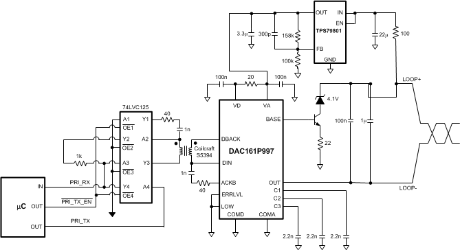
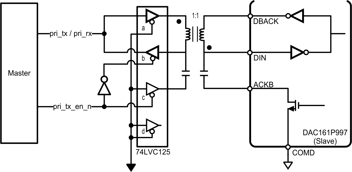 Figure 27. Typical SWIF Implementation
The interface implementation shown in Figure 27 can be expanded or simplified depending on the requirements of the system and capabilities of the Master controller. A number of other possible implementations are shown in the figures below.
Figure 28 shows the circuit analogous in its functionality to the circuit in Figure 27 but with fewer active components. Here instead of disabling ‘b’ buffer during data transmission, its output impedance is increased to the point where its drive is significant only during the data reception form the Slave.
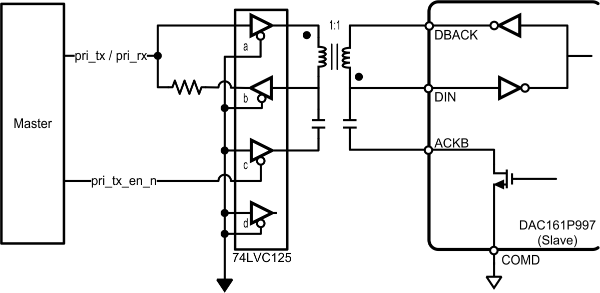 Figure 28. SWIF Link With Simplified Control
Figure 29 shows the SWIF link circuit when the Master does not have a bidirectional I/O available. The Master output driving pri_tx is split away from the Master receiving pri_rx input by using a buffer ‘d’, until now unused, on 74LVC125.
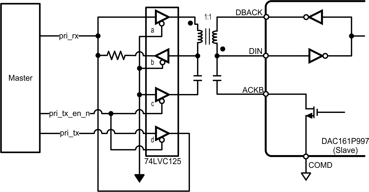 Figure 29. Master Without Bidirectional I/O
Figure 30 shows the trivial circuit realization of the SWIF link in simplex mode, unidirectional data flow.
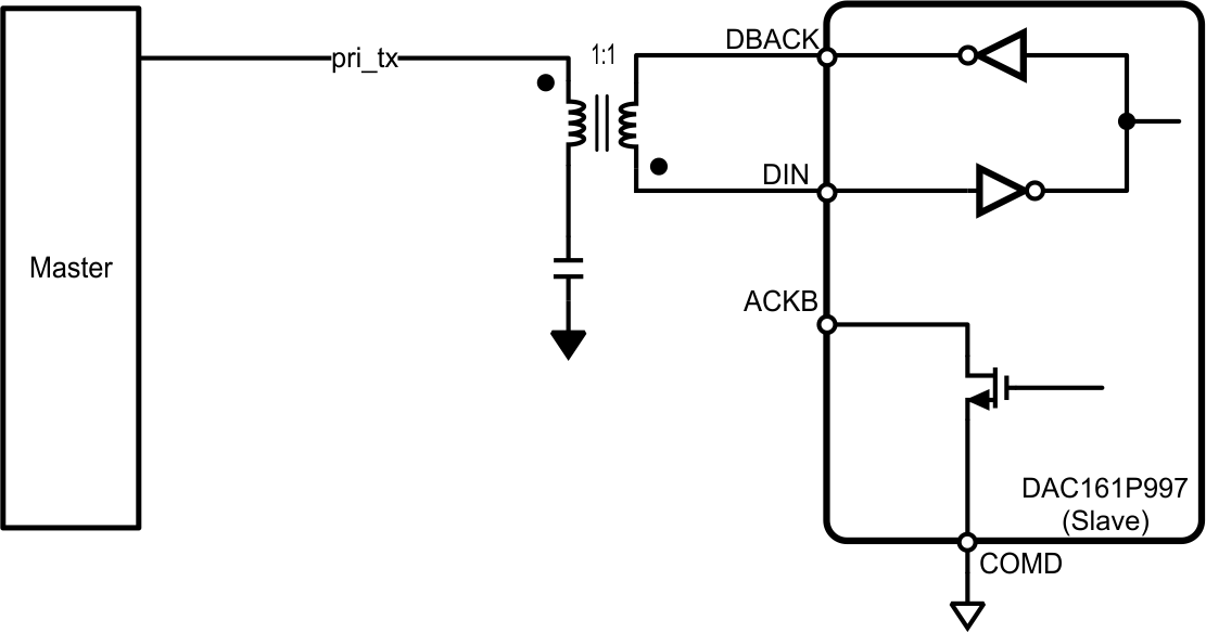 Figure 30. SWIF Without Acknowledge Capability
Figure 31 shows the DC coupled SWIF link realization. In this example ACKB output is used to generate the Acknowledge pulse. This is equivalent to the Acknowledge pulse generated at DBACK, since in transformer coupled application both ACKB and DBACK have to be pulsed to transmit back to the Master. Note that the pulse generated by ACKB is active LOW.
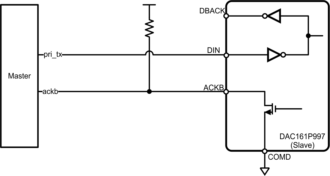 Figure 31. DC-Coupled SWIF Link
The SWIF link realization using opto-couplers (opto-isolators) is shown in Figure 32. Points of note here are: the opto-couplers invert the SWIF symbol waveform, and there is increased power consumption due to the relatively large currents required to turn on the internal diodes and standing current in the pull-up resistors.
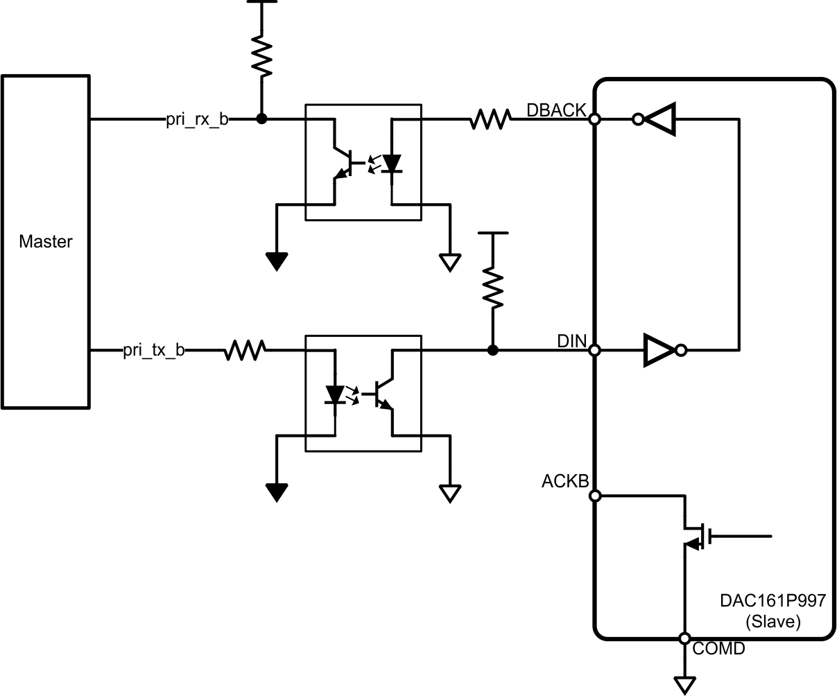 Figure 32. SWIF Link Realized With Octo-Couplers
8.2.3 Application Curve
Unless otherwise noted, these specifications apply for VA = VD = 3.3 V, COMA = COMD = 0 V, TA= 25°C, external bipolar transistor: 2N3904, RE = 22 Ω, C1 = C2 = C3 = 2.2 nF.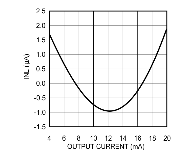 Figure 33. Linearity vs ILOOP