SNAS515G July 2011 – December 2014 DAC161P997
PRODUCTION DATA.
- 1 Features
- 2 Application
- 3 Description
- 4 Revision History
- 5 Pin Configuration and Functions
- 6 Specifications
- 7 Detailed Description
- 8 Application and Implementation
- 9 Power Supply Recommendations
- 10Layout
- 11Device and Documentation Support
- 12Mechanical, Packaging, and Orderable Information
Package Options
Mechanical Data (Package|Pins)
- RGH|16
Thermal pad, mechanical data (Package|Pins)
- RGH|16
Orderable Information
7 Detailed Description
7.1 Overview
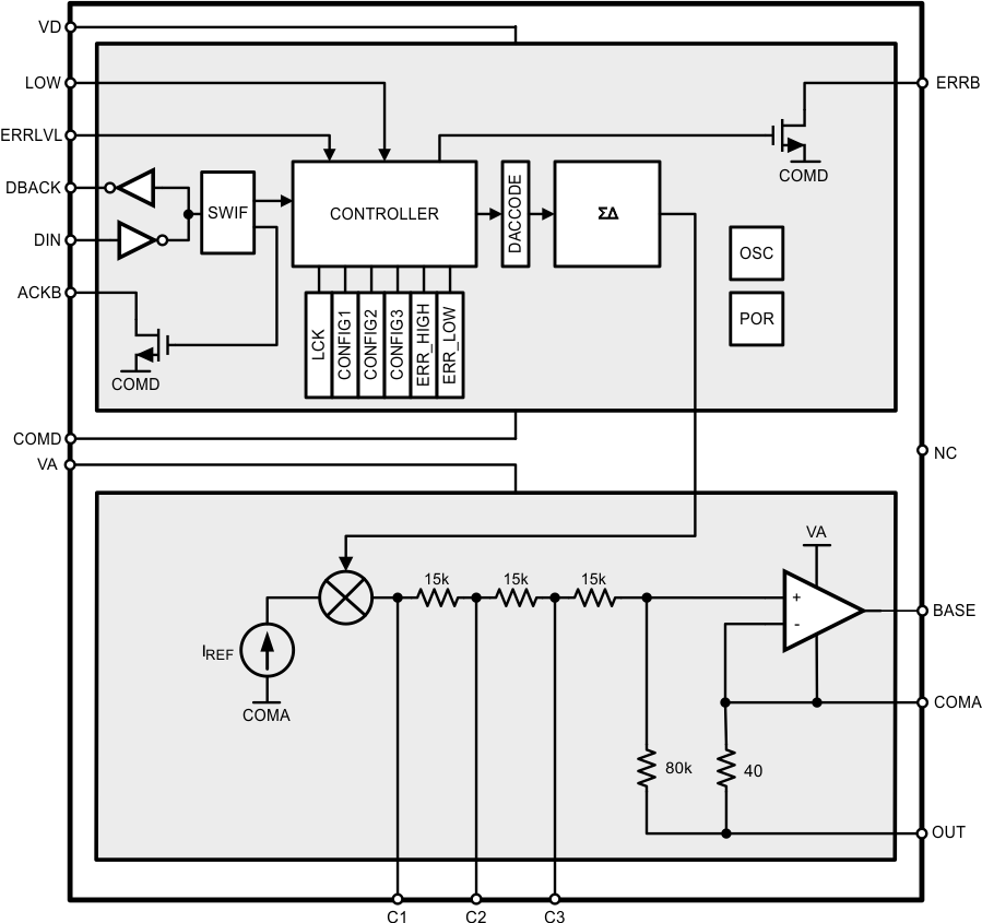
The DAC161P997 is a 16-bit DAC realized as a ∑Δ modulator. The DAC’s output is a current pulse train that is filtered by the on-board low pass RC filter. The final output current is a multiplied copy of the filtered modulator output. This architecture ensures an excellent linearity performance, while minimizing power consumption of the device.
The DAC161P997 eases the design of robust, precise, long-term stable industrial systems by integrating all precision elements on-chip. Only a few external components are needed to realize a low-power, high-precision industrial 4-20 mA transmitter.
In case of a fault, or during initial power-up the DAC161P997 will output current in either upper or lower error current band. The choice of band is user selectable via a device pin. The error current value is user programmable via the SWIF link by the Master.
7.2 Functional Block Diagram
7.3 Feature Description
7.3.1 Error Detection and Reporting
The user can modify the CONFIG2:(LOOP | CHANNEL | PARITY | FRAME) bits to mask or enable the reporting of any of the detectable fault conditions. The DAC161P997 reports errors by asserting the ERRB signal, and by setting the current sourced by OUT to a value dictated by the state at ERRLVL pin and the contents of the ERR_HIGH and ERR_LOW registers. Once the condition causing the fault is removed the OUT will return to the last valid output level prior to the occurrence of the fault.
Table 1 below summarizes the detectable faults, and means of reporting. The interval TM is governed by the internal timer and is specified in Electrical Characteristics.
Table 1. Error Detection and Reporting
| ERROR | CAUSE | REPORTING | |
|---|---|---|---|
| ERRB | Value used by the DAC to set OUT pin current | ||
| LOOP | The device cannot sustain the required output current at OUT pin, typically caused by drop in loop supply, or increased load impedance. | LOW | ERR_LOW |
| The DAC161P997 automatically clears this fault after interval of TM and attempts to establish output current dictated by the value in the DACCODE register | |||
| CHANNEL | no valid symbols have been received on DIN in last interval of TM | LOW | ERRLVL=1: ERR_HIGH |
| ERRLVL=0: ERR_LOW | |||
| PARITY | SWIF received a valid data frame, but a bit error has been detected by parity check | LOW | ERRLVL=1: ERR_HIGH |
| ERRLVL=0: ERR_LOW | |||
| FRAME | invalid symbol received, or an incorrect number of valid symbols were detected in the frame | LOW | ERRLVL=1: ERR_HIGH |
| ERRLVL=0: ERR_LOW | |||
7.3.2 Alarm Current
The DAC161P997 reports faults to the plant controller by forcing the OUT current into one of the error bands. The error current bands are defined as either above 20 mA, or below 4mA. The error band selection is done via the ERRLVL pin. The exact value of the output current used to indicate fault is dictated by the contents of ERR_HIGH and ERR_LOW registers. See ERR_LOW and ERR_HIGH.
The default settings for LOW ERROR CURRENT and HIGH ERROR CURRENT are specified in Electrical Characteristics
7.4 Device Functional Modes
SWIF is a versatile and robust solution for transmitting digital data over the galvanic isolation boundary using just one isolation element: a pulse transformer.
Digital data format achieves the information transmission without the loss of fidelity which usually afflicts transmissions employing PWM (Pulse Width Modulation) schemes. Digital transmission format also makes possible data differentiation: user can specify whether given data word is a DAC input to be converted to loop current, or it is a device configuration word.
SWIF was designed to use in conjunction with pulse transformer as an isolation element. The use of the transformers to cross the isolation boundary is typical in the legacy systems due to their robustness, low-power consumption, and low cost. However, system implementation is not limited to the transformer as a link since SWIF easily interfaces with opto-couplers, or it can be directly driven by a CMOS gate.
SWIF incorporates a number of features that address robustness aspect of the data link design:
-
Bidirectional signal flow the DAC161P997 can issue an ACKNOWLEDGE pulse back to the master transmitter, via the same physical channel, to confirm the reception of the valid data;
-
Error Detection SWIF protocol incorporates frame length detection and parity checks as a method of verifying the integrity of the received data;
-
Channel Activity DetectionSWIF can monitor the data channel and raise an error flag should the expected activity drop below programmable threshold, due to , for example, damage to the physical channel.
In the typical system the Master is a micro controller. SWIF has been implemented on a number of popular micro controllers where it places minimum demands on the hardware or software resources even of the simple 8-bit devices.
SWIF gives the system designer flexibility is balancing the trade-offs between the data rate, activity monitoring functionality and the power consumption in the transformer coupled data channel. At lowest data rates, with long inactive inter-frame periods, the power consumed by SWIF is negligible. See Inter-Frame Period.
7.5 Programming
7.5.1 Single-Wire Interface (SWIF)
SWIF provides flexible and easy to implement digital data link between the Master (transmitter) and the Slave (receiver). The Master encodes the digital data into a square (NRZ) CMOS level waveform which can be generated using common microcontroller resources. The Slave (DAC161P997) translates the waveform back into a bit stream which is then interpreted as the output current update or configuration data.
SWIF can operate in both Simplex (unidirectional) and Half-Duplex (bidirectional) modes. In the DAC161P997's implementation of SWIF, an Acknowledge pulse constitutes the reverse data flowing from the Slave back to the Master.
In its simplest implementation, the waveform can be directly coupled to the DAC161P997 input. In typical systems, however, SWIF data is transmitted via the galvanic isolation element such as pulse transformer or an opto-coupler. The details of the circuit implementations are discussed in Interface Circuit.
Frame Formatthrough Symbol Set describe the data encoding and the SWIF protocol.
7.5.1.1 Frame Format
A frame begins with a minimum of one idle symbol. There can be more than one and each has the effect of resetting the frame buffer of the DAC161P997. After idle symbol “D” a Tag Bit specifies the destination of the frame. If the tag is symbol ‘0’ then frame’s destination is the DACCODE register. If tag is a ‘1’ the destination is one of the configuration registers.
The following 16 symbols constitute the data payload. If current frame is a DAC frame, the entire payload is a single DACCODE word. If it is a configuration frame, the first byte is the register address and the second byte is the register data. Words are transmitted MSB first.
Two parity symbols follow the payload. The first parity symbol is determined by the bit parity of the tag bit and the first byte of payload (HIGH Slice) – a total of nine symbols. The second parity symbol corresponds to bit parity of the second byte of payload only (LOW Slice) – a total of 8 symbols.
P0 = [ ( Number of ones in LOW Slice ) mod 2 == 0 ]
P1 = [ ( Number of ones in HIGH Slice ) mod 2 == 0 ]
Symbol ‘D’ after the parity bits completes a valid frame.
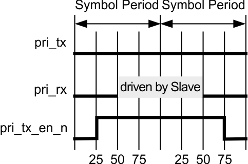
The symbol “A” is optional, but if present it has to immediately follow the last “D” symbol of the frame. The duration of acknowledge symbol “A” is always twice the duration of P0 symbol preceding it. See Figure 12.
SWIF does not require that all symbols in valid frames are sent by the Master at a fixed Baud rate. Each symbol is evaluated individually and is recognized as valid as long as it conforms to the duration requirement (Tp) and its duty cycle falls outside of noise margins. (See Table 2 below.)
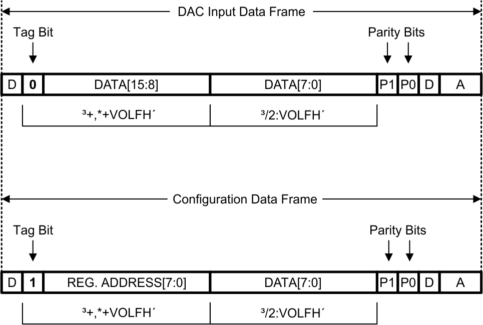 Figure 12. Data Frame Format
7.5.1.2 Inter-Frame Period
The fastest DAC update rate is achieved when Master sends the valid frames back to back, Continuous Mode, at the fastest Baud rate. This, however, results in the least power efficient implementation.

SWIF is designed to operate in the Burst Mode as well, where the valid frames are separated by the inter-frame periods that do not carry any data. The inter-frame period can be occupied by a stream of idle ‘D’ or ‘L’ symbols.
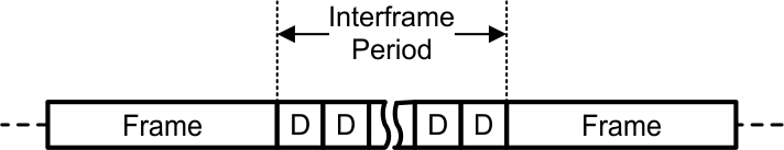
Sending the ‘D’ symbol in the inter-frame period provides continuous verification of integrity of the data link. The device by default monitors the activity of the SWIF link, and if the activity ceases the ERRB flag is asserted. See CONFIG2 and Error Detection and Reporting.
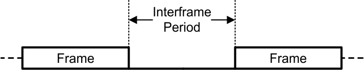
Sending the ‘L’ in the inter-frame period results in the transmission line being inactive (transition-free) except when the data frames are being transmitted. This is the most power efficient implementation of SWIF link, but it does not facilitate link integrity reporting. To avoid ERRB being asserted due to the channel inactivity, CONFIG2.CHANNEL should be cleared.
7.5.1.3 Symbol Set
The digital data encoding scheme is outlined in the table below. The signal names in the table correspond to the nodes shown in Figure 27.
The signal waveforms due to a random symbol stream are shown in Figure 13.
Table 2. Symbol Set Table
| Character Mnemonic | SWIF Symbol | Comments |
|---|---|---|
| “0” |
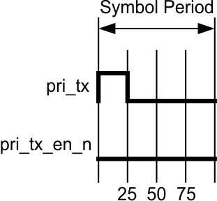 |
|
| “1” |
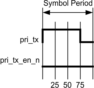 |
|
| “D” |
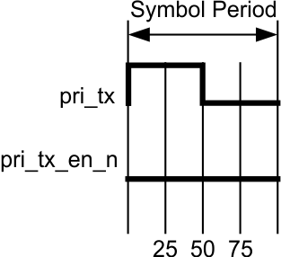 |
|
| “A” |
 |
|
| “L” |
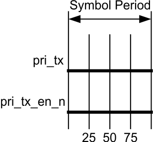 |
|
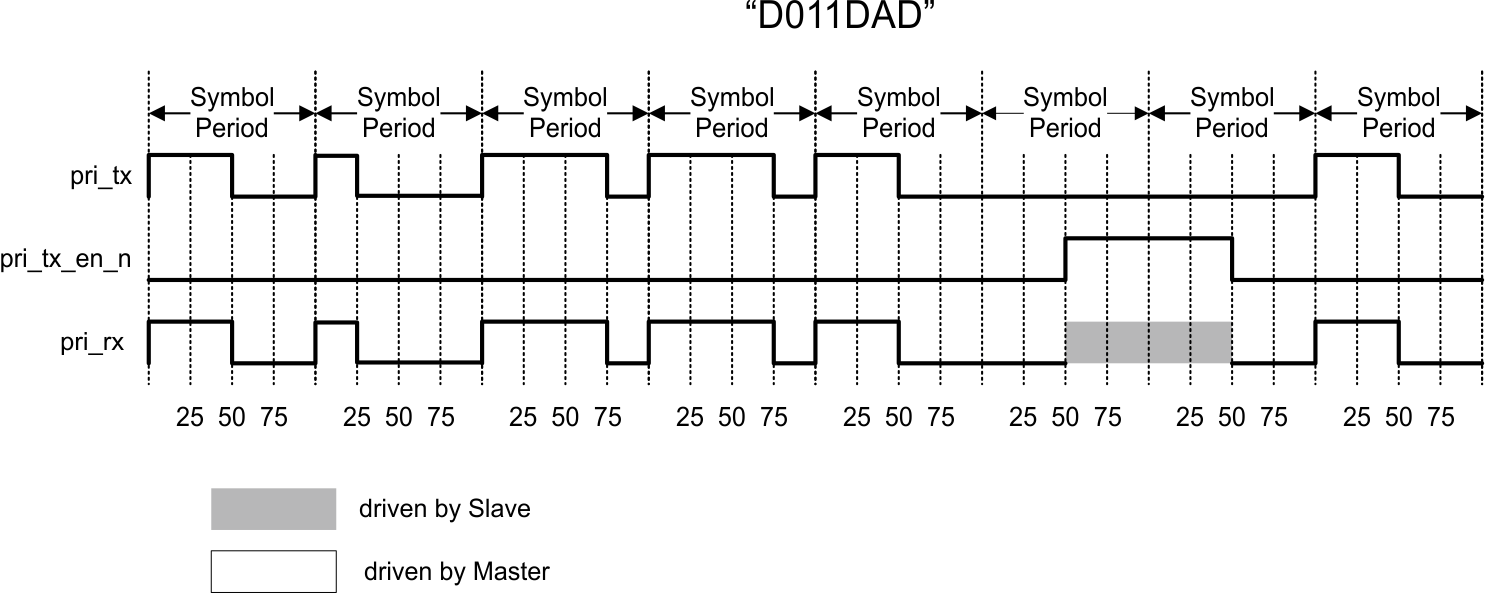 Figure 13. Symbol Stream Example
7.5.1.4 Interface Circuit
SWIF interface components are shown in Figure 14. The buffers A and B comprise a square waveform recovery circuit in applications where a pulse transformer is used to cross the galvanic isolation boundary, see Transformer Coupled Interface - Data Flow to the DAC. The ACKB output and its internal NMOS switch provide the means of reversing the direction of data flow through the coupling transformer see Transformer Coupled Interface - Acknowledge Pulse. In simple cases where the data link is DC coupled buffer A alone acts as a data receiver. The buffer C is provided for cases where improved noise immunity is required, see DC-Coupled Interface.
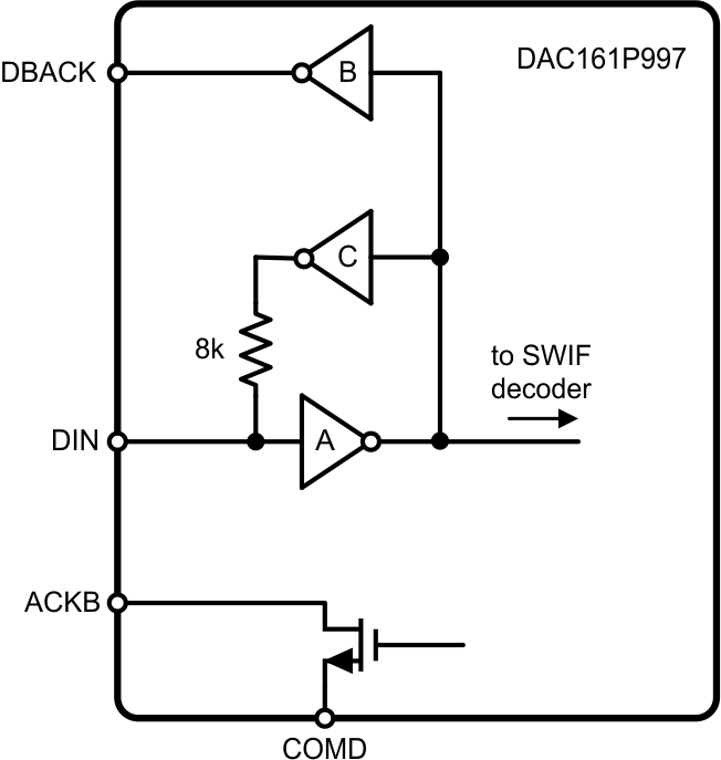 Figure 14. SWIF Front End
7.5.1.4.1 Transformer Coupled Interface - Data Flow to the DAC
In systems requiring galvanic isolation between the transmitter (micro-controller) and the receiver, the commonly used coupling element is a pulse transformer. Transformer passes only the AC components of the square input waveform resulting in an impulse train across the secondary winding. Buffers A and B form a latch circuit around the secondary winding that recovers the square waveform from the impulse train.
Figure 15 shows the details of the square waveform transmission from the primary side and recovery of the signal on the secondary side. Transmitter’s DC component is blocked by the capacitor CP. The transmitter’s output waveform VO results in the impulse train VP across the primary winding. Similar impulse train then appears across the secondary winding. If the magnitude of the impulse exceeds the threshold on the A buffer, the latch formed by A and B buffers will change state. The new latch state will persist until an opposite polarity impulse appears across the secondary winding.
Note that in Figure 15 the capacitor CS bottom plate floats, and thus does not affect the operation of this circuit.
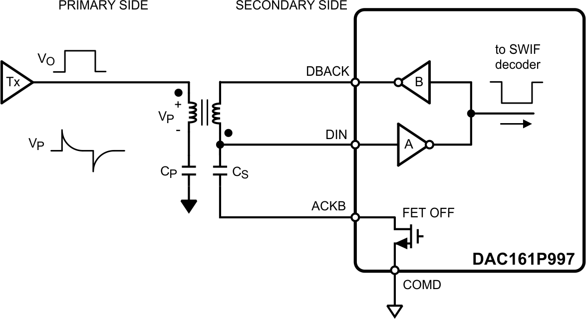 Figure 15. Transformer-Coupled SWIF Link With the DAC161P997 as Receiver
7.5.1.4.2 Transformer Coupled Interface - Acknowledge Pulse
Since the transformer is a symmetrical device (particularly one with 1:1 winding ratio), it is simple to reverse the data flow through it.
Figure 16 shows the SWIF interface circuit during the transmission of the Acknowledge pulse from the DAC161P997 on the secondary side back to the micro-controller on the primary side.
On the secondary side buffer B drives the square waveform across the transformer. Capacitor CS, whose bottom plate is now grounded via the ACKB pin, blocks the DC component of the square waveform. Buffer A is inactive.
On the primary side a square waveform recovery is performed by the now familiar latch.
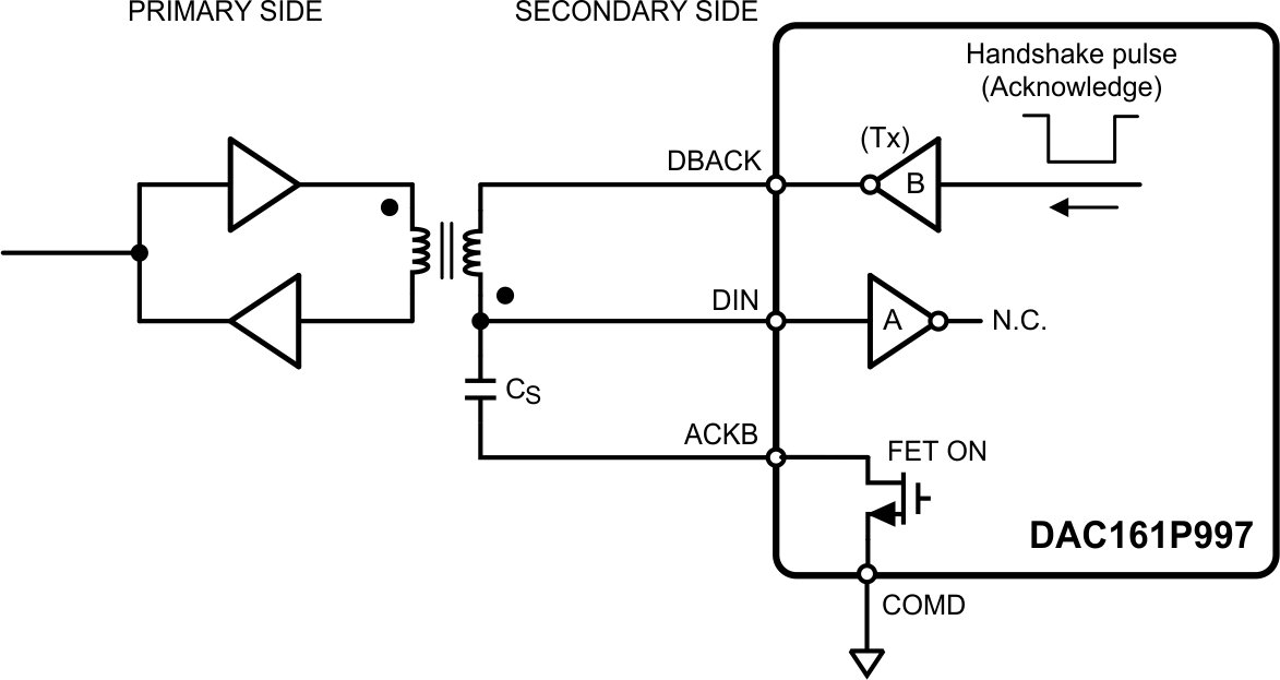 Figure 16. Transformer-Coupled SWIF Link With the DAC161P997 as Transmitter
7.5.1.4.3 DC-Coupled Interface
DC coupled signal path between the transmitter and the receiver is shown in Figure 17. Such circuit as the internal buffer A is sufficient for the signal recovery as the signal presented at the DIN input is a square CMOS level waveform.
In noisy environments it may be necessary to implement a Hysteresis loop around the DIN input to improve noise immunity of the input circuit. Presence of the buffer C and its output resistor facilitate this. The Hysteresis can be easily realized by inserting RIN between the transmitter and DIN input.
Note that when RIN = 0 the presence of the buffer C can be ignored.
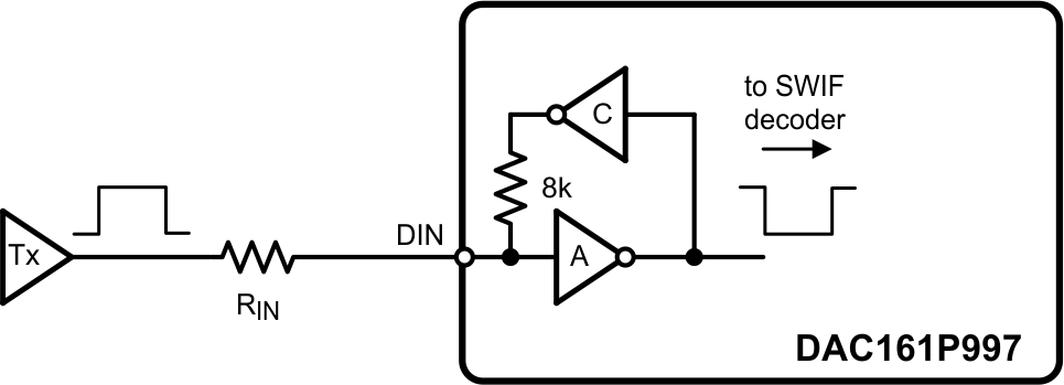 Figure 17. DC-Coupled SWIF Input
7.5.1.4.4 Transformer Selection and SWIF Data Link Circuit Design
In general, the transformers developed for T1/E1 telecom applications are well suited as the interface element for the DAC161P997 in the galvanically isolated industrial transmitter. The application circuit schematic utilizing T1/E1 transformer as the isolation element is shown in Typical Application. A number of suggested off the shelf transformers are listed in Table 3.
Table 3. Examples of Transformers Suitable in the DAC161P997 Applications
Model suitable for simulating the behavior of the pulse transformer is shown in Figure 18. The model parameters are readily available in the datasheets provided by the transformer manufacturers, see Table 3 for examples.
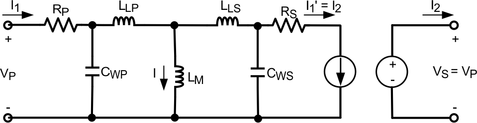 Figure 18. Pulse Transformer Model - Winding Ratio 1:1
Table 4. Transformer Model Parameters' Legend
| Parameter | Description |
|---|---|
| LM | Magnetizing inductance, in Data Sheets shown as OCL (open circuit inductance) |
| LLP/S | Leakage inductance of the primary (secondary) winding |
| CWP/S | Winding capacitance. Dominated by the CWW (winding to winding) component. Here it is assumed that CWS=CWP=½CWW |
| RP/S | Winding resistance |
The circuit behavior will be dominated by the DC blocking capacitance CP and the magnetizing inductance LM. In the example circuit shown in Figure 19 the rising edge of VO ultimately results in an impulse at the input DIN, see Figure 20. Once voltage at DIN is above VIH of the A buffer, the A buffer will change its state. However, the latch will acquire a new state only if the voltage at DIN persists above VIH for TPEAK > TD.
The parasitic elements in the transformer model: LLS, LSP, CWS, CWP may result in the oscillating component superimposed on the dominant impulse response waveform shown in Figure 20. The oscillation should be controlled so that the condition TPEAK> TD is maintained. The typical method for controlling this parasitic oscillation is to insert a damping element into the signal path. A small resistance in series with transformer winding is such damping element. The typical application example in Typical Application illustrates this.
The delay around the SWIF input latch, from DIN to DBACK, TD is specified in Electrical Characteristics.
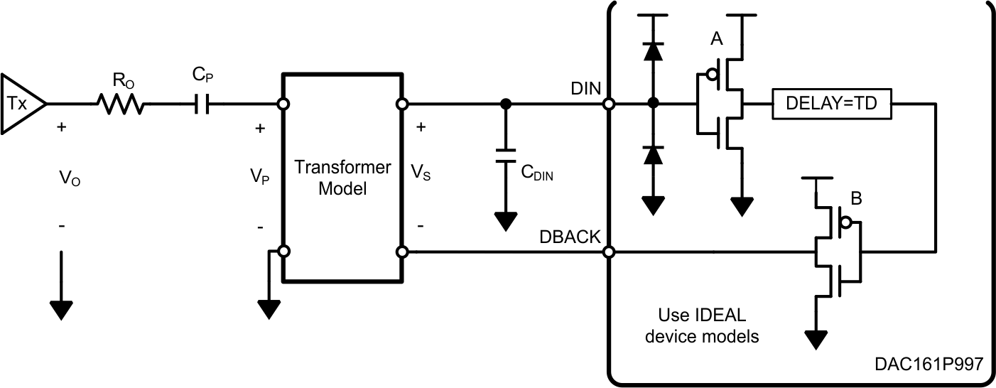 Figure 19. NRZ Waveform Transmission and Recovery Circuit Model
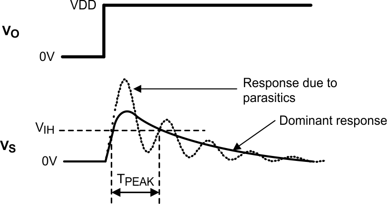 Figure 20. SWIF Link Circuit Response to Step-Input
7.6 Register Maps
7.6.1 LCK
| Address=0x00; Default=0x00 | ||
|---|---|---|
| Bit Field | Name | Description |
| 7:0 | 0x95 - registers unlocked 0x** - any value written locks registers A register lock prevents inadvertent changes to the configuration. The DAC output cannot be updated while software configuration registers are unlocked. |
|
7.6.2 CONFIG1
| Address=0x01; Default=0x08 | ||
|---|---|---|
| Bit Field | Name | Description |
| 7:5 | RESERVED. Always write 0. | |
| 4:3 | SERR | 0b00 - NOP 0b01 - set error 0b10 - clear error 0b11 - NOP Sets or clears the error condition. At power-on the error is set. Error is also cleared after reception of valid SWIF frame. These bits are self clearing. This functionality can be used for diagnostic purposes, e.g. Master can use SERR to force ILOOP into an error band, and then return it to previously held output level. |
| 2:1 | RESERVED. Always write 0. | |
| 0 | RST | 0 - NOP 1- same as power-on reset. Once device is reset to default state the bit clears automatically |
7.6.3 CONFIG2
| Address=0x02; Default=0x1F | ||
|---|---|---|
| Bit Field | Name | Description |
| 7:5 | RESERVED. Always write 0. | |
| 4 | ACK_EN | Set to enable ACK When enabled, an acknowledgement is indicated on the serial interface upon detection of each valid frame. See Frame Format. |
| 3 | FRAME | Set to enable framing error reporting. See table in Error Detection and Reporting. |
| 2 | PARITY | Set to enable parity error reporting. See table in Error Detection and Reporting. |
| 1 | CHANNEL | Set to enable channel-inactive reporting. See table in Error Detection and Reporting. |
| 0 | LOOP | Set to enable loop error reporting. See table in Error Detection and Reporting. |
7.6.4 CONFIG3
| Address=0x03; Default=0x08 | ||
|---|---|---|
| Bit Field | Name | Description |
| 7:4 | RESERVED. Always write 0. | |
| 3:0 | RX_ERR_CNT | 0 <= RX_ERR_CNT ≤ 15 Threshold = 1 + RX_ERR_CNT The slave enters the error state once ‘Threshold’ number of consecutive FRAME or PARITY errors are counted. The threshold is programmable to prevent occasional errors from being reported. See table in Error Detection and Reporting. |
7.6.5 ERR_LOW
| Address=0x04; Default=0x24 | ||
|---|---|---|
| Bit Field | Name | Description |
| 7:0 | 8-bit value. If ERRLVL = LOW, the DAC will use the value stored in ERR_LOW register to set the output current sourced from OUT pin when reporting an error condition. The ERR_LOW value is used as the upper byte of the DACCODE, while the lower byte is forced to 0x00. At power up the ERR_LOW defaults to a value which forces IERRL output current. See Electrical Characteristics. | |
7.6.6 ERR_HIGH
| Address=0x05; Default=0xE8 | ||
|---|---|---|
| Bit Field | Name | Description |
| 7:0 | If ERRLVL = HIGH, the DAC will use the value stored in ERR_HIGH register to set the output current sourced from OUT pin when reporting an error condition. The ERR_HIGH value is used as the upper byte of the DACCODE, while the lower byte is forced to 0x00. At power-up the ERR_HIGH defaults to a value which forces IERRH output current. See Electrical Characteristics. | |