SLASE47 January 2015 DAC39J82
PRODUCTION DATA.
- 1 Features
- 2 Applications
- 3 Description
- 4 Revision History
- 5 Pin Configuration and Functions
- 6 Specifications
-
7 Detailed Description
- 7.1 Overview
- 7.2 Functional Block Diagram
- 7.3
Feature Description
- 7.3.1 Serdes Input
- 7.3.2 Serdes Rate
- 7.3.3 Serdes PLL
- 7.3.4 Serdes Equalizer
- 7.3.5 JESD204B Descrambler
- 7.3.6 JESD204B Frame Assembly
- 7.3.7 Serial Peripheral Interface (SPI)
- 7.3.8 Multi-Device Synchronization
- 7.3.9 Input Multiplexer
- 7.3.10 FIR Filters
- 7.3.11 Full Complex Mixer
- 7.3.12 Coarse Mixer
- 7.3.13 Dithering
- 7.3.14 Quadrature Modulation Correction (QMC)
- 7.3.15 Group Delay Correction Block
- 7.3.16 Output Multiplexer
- 7.3.17 Power Measurement And Power Amplifier Protection
- 7.3.18 Serdes Test Modes
- 7.3.19 Error Counter
- 7.3.20 Eye Scan
- 7.3.21 JESD204B Pattern Test
- 7.3.22 Temperature Sensor
- 7.3.23 Alarm Monitoring
- 7.3.24 LVPECL Inputs
- 7.3.25 CMOS Digital Inputs
- 7.3.26 Reference Operation
- 7.3.27 Analog Outputs
- 7.3.28 DAC Transfer Function
- 7.4 Device Functional Modes
- 7.5
Register Map
- 7.5.1
Register Descriptions
- 7.5.1.1 config0 Register - Address: 0x00, Default: 0x0218
- 7.5.1.2 config1 Register - Address: 0x01, Default: 0x0003
- 7.5.1.3 config2 Register - Address: 0x02, Default: 0x2002
- 7.5.1.4 config3 Register - Address: 0x03, Default: 0xF380
- 7.5.1.5 config4 Register - Address: 0x04, Default: 0x00FF
- 7.5.1.6 config5 Register - Address: 0x05, Default: 0xFFFF
- 7.5.1.7 config6 Register - Address: 0x06, Default: 0xFFFF
- 7.5.1.8 config7 Register - Address: 0x07, Default: 0x0000
- 7.5.1.9 config8 Register - Address: 0x08, Default: 0x0000
- 7.5.1.10 config9 Register - Address: 0x09, Default: 0x0000
- 7.5.1.11 config10 Register - Address: 0x0A, Default: 0x0000
- 7.5.1.12 config11 Register - Address: 0x0B, Default: 0x0000
- 7.5.1.13 config12 Register - Address: 0xC, Default: 0x0400
- 7.5.1.14 config13 Register - Address: 0xD, Default: 0x0400
- 7.5.1.15 config14 Register - Address: 0x0E, Default: 0x0400
- 7.5.1.16 config15 Register - Address: 0x0F, Default: 0x0400
- 7.5.1.17 config16 Register - Address: 0x10, Default: 0x0000
- 7.5.1.18 config17 Register - Address: 0x11, Default: 0x0000
- 7.5.1.19 config18 Register - Address: 0x12, Default: 0x0000
- 7.5.1.20 config19 Register - Address: 0x13, Default: 0x0000
- 7.5.1.21 config20 Register - Address: 0x14, Default: 0x0000
- 7.5.1.22 config21 Register - Address: 0x15, Default: 0x0000
- 7.5.1.23 config22 Register - Address: 0x16, Default: 0x0000
- 7.5.1.24 config23 Register - Address: 0x17, Default: 0x0000
- 7.5.1.25 config24 Register - Address: 0x18, Default: 0x0000
- 7.5.1.26 config25 Register - Address: 0x19, Default: 0x0000
- 7.5.1.27 config26 Register - Address: 0x1A, Default: 0x0020
- 7.5.1.28 config27 Register - Address: 0x1B, Default: 0x0000
- 7.5.1.29 config28 Register - Address: 0x1C, Default: 0x0000
- 7.5.1.30 config29 Register - Address: 0x1D, Default: 0x0000
- 7.5.1.31 config30 Register - Address: 0x1E, Default: 0x1111
- 7.5.1.32 config31 Register - Address: 0x1F, Default: 0x1111
- 7.5.1.33 config32 Register - Address: 0x20, Default: 0x0000
- 7.5.1.34 config33 Register - Address: 0x21, Default: 0x0000
- 7.5.1.35 config34 Register - Address: 0x22, Default: 0x1B1B
- 7.5.1.36 config35 Register - Address: 0x23, Default: 0xFFFF
- 7.5.1.37 config36 Register - Address: 0x24, Default: 0x0000
- 7.5.1.38 config37 Register - Address: 0x25, Default: 0x8000
- 7.5.1.39 config38 Register - Address: 0x26, Default: 0x0000
- 7.5.1.40 config39 Register - Address: 0x27, Default: 0x0000
- 7.5.1.41 config40 Register - Address: 0x28, Default: 0x0000
- 7.5.1.42 config41 Register - Address: 0x29, Default: 0x0000
- 7.5.1.43 config42 Register - Address: 0x2A, Default: 0x0000
- 7.5.1.44 config43 Register - Address: 0x2B, Default: 0x0000
- 7.5.1.45 config44 Register - Address: 0x2C, Default: 0x0000
- 7.5.1.46 config45 Register - Address: 0x2D, Default: 0x0000
- 7.5.1.47 config46 Register - Address: 0x2E, Default: 0xFFFF
- 7.5.1.48 config47 Register - Address: 0x2F, Default: 0x0004
- 7.5.1.49 config48 Register - Address: 0x30, Default: 0x0000
- 7.5.1.50 config49 Register - Address: 0x31, Default: 0x0000
- 7.5.1.51 config50 Register - Address: 0x32, Default: 0x0000
- 7.5.1.52 config51 Register - Address: 0x33, Default: 0x0100
- 7.5.1.53 config52 Register - Address: 0x34, Default: 0x0000
- 7.5.1.54 config53 Register - Address: 0x35, Default: 0x0000
- 7.5.1.55 config54 Register - Address: 0x36, Default: 0x0000
- 7.5.1.56 config55 Register - Address: 0x37, Default: 0x0000
- 7.5.1.57 config56 Register - Address: 0x38, Default: 0x0000
- 7.5.1.58 config57 Register - Address: 0x39, Default: 0x0000
- 7.5.1.59 config58 Register - Address: 0x3A, Default: 0x0000
- 7.5.1.60 config59 Register - Address: 0x3B, Default: 0x0000
- 7.5.1.61 config60 Register - Address: 0x3C, Default: 0x0000
- 7.5.1.62 config61 Register - Address: 0x3D, Default: 0x0000
- 7.5.1.63 config62 Register - Address: 0x3E, Default: 0x0000
- 7.5.1.64 config63 Register - Address: 0x3F, Default: 0x0000
- 7.5.1.65 config64 Register - Address: 0x40, Default: 0x0000
- 7.5.1.66 config65 Register - Address: 0x41, Default: 0x0000
- 7.5.1.67 config66 Register - Address: 0x42, Default: 0x0000
- 7.5.1.68 config67 Register - Address: 0x43, Default: 0x0000
- 7.5.1.69 config68 Register - Address: 0x44, Default: 0x0000
- 7.5.1.70 config69 Register - Address: 0x45, Default: 0x0000
- 7.5.1.71 config70 Register - Address: 0x46, Default: 0x0120
- 7.5.1.72 config71 Register - Address: 0x47, Default: 0x3450
- 7.5.1.73 config72 Register - Address: 0x48, Default: 0x31C3
- 7.5.1.74 config73 Register - Address: 0x49, Default: 0x0000
- 7.5.1.75 config74 Register - Address: 0x4A, Default: 0x001E
- 7.5.1.76 config75 Register - Address: 0x4B, Default: 0x0000
- 7.5.1.77 config76 Register - Address: 0x4C, Default: 0x0000
- 7.5.1.78 config77 Register - Address: 0x4D, Default: 0x0300
- 7.5.1.79 config78 Register - Address: 0x4E, Default: 0x0F0F
- 7.5.1.80 config79 Register - Address: 0x4F, Default: 0x1CC1
- 7.5.1.81 config80 Register - Address: 0x50, Default: 0x0000
- 7.5.1.82 config81 Register - Address: 0x51, Default: 0x00FF
- 7.5.1.83 config82 Register - Address: 0x52, Default: 0x00FF
- 7.5.1.84 config83 Register - Address: 0x53, Default: 0x0000
- 7.5.1.85 config84 Register - Address: 0x54, Default: 0x00FF
- 7.5.1.86 config85 Register - Address: 0x55, Default: 0x00FF
- 7.5.1.87 config86 Register - Address: 0x56, Default: 0x0000
- 7.5.1.88 config87 Register - Address: 0x57, Default: 0x00FF
- 7.5.1.89 config88 Register - Address: 0x58, Default: 0x00FF
- 7.5.1.90 config89 Register - Address: 0x59, Default: 0x0000
- 7.5.1.91 config90 Register - Address: 0x5A, Default: 0x00FF
- 7.5.1.92 config91 Register - Address: 0x5B, Default: 0x00FF
- 7.5.1.93 config92 Register - Address: 0x5C, Default: 0x1111
- 7.5.1.94 config93 Register - Address: 0x5D, Default: 0x0000
- 7.5.1.95 config94 Register - Address: 0x5E, Default: 0x0000
- 7.5.1.96 config95 Register - Address: 0x5F, Default: 0x0123
- 7.5.1.97 config96 Register - Address: 0x60, Default: 0x4567
- 7.5.1.98 config97 Register - Address: 0x61, Default: 0x000F
- 7.5.1.99 config98 Register - Address: 0x62, Default: 0x0000
- 7.5.1.100 config99 Register - Address: 0x63, Default: 0x0000
- 7.5.1.101 config100 Register - Address: 0x64, Default: 0x0000
- 7.5.1.102 config101 Register - Address: 0x65, Default: 0x0000
- 7.5.1.103 config102 Register - Address: 0x66, Default: 0x0000
- 7.5.1.104 config103 Register - Address: 0x67, Default: 0x0000
- 7.5.1.105 config104 Register - Address: 0x68, Default: 0x0000
- 7.5.1.106 config105 Register - Address: 0x69, Default: 0x0000
- 7.5.1.107 config106 Register - Address: 0x6A, Default: 0x0000
- 7.5.1.108 config107 Register - Address: 0x6B, Default: 0x0000
- 7.5.1.109 config108 Register - Address: 0x6C, Default: 0x0000
- 7.5.1.110 config109 Register - Address: 0x6D, Default: 0x00xx
- 7.5.1.111 config110 Register - Address: 0x6E, Default: 0x0000
- 7.5.1.112 config111 Register - Address: 0x6F, Default: 0x0000
- 7.5.1.113 config112 Register - Address: 0x70, Default: 0x0000
- 7.5.1.114 config113 Register - Address: 0x71, Default: 0x0000
- 7.5.1.115 config114 Register - Address: 0x72, Default: 0x0000
- 7.5.1.116 config115 Registe - Address: 0x73, Default: 0x0000
- 7.5.1.117 config116 Register - Address: 0x74, Default: 0x0000
- 7.5.1.118 config117 Register - Address: 0x75, Default: 0x0000
- 7.5.1.119 config118 Register - Address: 0x76, Default: 0x0000
- 7.5.1.120 config119 Register - Address: 0x77, Default: 0x0000
- 7.5.1.121 config120 Register - Address: 0x78, Default: 0x0000
- 7.5.1.122 config121 Register - Address: 0x79, Default: 0x0000
- 7.5.1.123 config122 Register - Address: 0x7A, Default: 0x0000
- 7.5.1.124 config123 Register - Address: 0x7B, Default: 0x0000
- 7.5.1.125 config124 Register - Address: 0x7C, Default: 0x0000
- 7.5.1.126 config125 Register - Address: 0x7D, Default: 0x0000
- 7.5.1.127 config126 Register - Address: 0x7E, Default: 0x0000
- 7.5.1.128 config127 Register - Address: 0x7F, Default: 0x0009
- 7.5.1
Register Descriptions
- 8 Applications and Implementation
- 9 Power Supply Recommendations
- 10Layout
- 11Device and Documentation Support
- 12Mechanical, Packaging, and Orderable Information
Package Options
Mechanical Data (Package|Pins)
- AAV|144
Thermal pad, mechanical data (Package|Pins)
Orderable Information
7 Detailed Description
7.1 Overview
The DAC39J82 is a very low power, 16-bit, 2.8 GSPS digital-to-analog converter (DAC) with JESD204B interface up to 12.5 Gbps. The maximum input data rate is 1.4 GSPS. The DAC39J82 is also pin-compatible with the 16-bit, dual-channel, 1.6/2.5 GSPS DAC37J82/DAC38J82.
Digital data is input to the device through 1, 2, 4 or 8 configurable serial JESD204B lanes running up to 12.5 Gbps with on-chip termination and programmable equalization. The interface allows JESD204B Subclass 1 SYSREF based deterministic latency and full synchronization of multiple devices.
The device includes features that simplify the design of complex transmit architectures. Fully bypassable 2x to 16x digital interpolation filters with over 90 dB of stop-band attenuation simplify the data interface and reconstruction filters. An on-chip 48-bit Numerically Controlled Oscillator (NCO) and independent complex mixers allow flexible and accurate carrier placement. A high-performance low jitter PLL simplifies clocking of the device without significant impact on the dynamic range. The digital Quadrature Modulator Correction (QMC) and Group Delay Correction (GDC) enable complete wideband IQ compensation for gain, offset, phase, and group delay between channels in direct up-conversion applications. A programmable Power Amplifier (PA) protection mechanism is available to provide PA protection in cases when the abnormal power behavior of the input data is detected.
DAC39J82 provides four analog outputs, and the data from the internal two digital paths can be routed to any two out of these four DAC outputs via the output multiplexer.
7.2 Functional Block Diagram
7.3 Feature Description
7.3.1 Serdes Input
The RX[7:0]P/N differential inputs are each internally terminated to a common point via 50 Ω, as shown in
Figure 55.
 Figure 55. Serial Lane Input Termination
Common mode termination is via a 50-pF capacitor to GND. The common mode voltage and termination of the differential signal can be controlled in a number of ways to suit a variety of applications via rw_cfgrx0 [10:8] (TERM), as described in Table 1.
(Note: AC coupling is recommended for JESD204B compliance.)
Table 1. Receiver Termination Selection
| TERM | EFFECT |
|---|---|
| 000 | Reserved |
| 001 | Common point set to 0.7 V. This configuration is for AC coupled systems. The transmitter has no effect on the receiver common mode, which is set to optimize the input sensitivity of the receiver. |
| 01x | Reserved |
| 100 | Common point set to GND. This configuration is for applications that require a 0-V common mode. |
| 101 | Common point set to 0.25 V. This configuration is for applications that require a low common mode. |
| 110 | Reserved |
| 111 | Common point floating. This configuration is for DC coupled systems in which the common mode voltage is set by the attached transmit link parter to 0 and 0.6 V. Note: this mode is not compatible with JESD204B. |
Data input is sampled by the differential sensing amplifier using clocks derived from the clock recovery algorithm. The polarity of RXP and RXN can be inverted by setting the INVPAIR [7:0] bit of the corresponding lane to “1”. This can potentially simplify PCB layout and improve signal integrity by avoiding the need to swap over the differential signal traces.
Due to processing effects, the devices in the RXP and RXN differential sense amplifiers will not be perfectly matched and there will be some offset in switching threshold. DAC39J82 contains circuitry to detect and correct for this offset. This feature can be enabled by setting the rw_cfgrx0 [23] (ENOC) bit to “1”. It is anticipated the most users will enable this feature. During the compensation process, rw_cfgrx0 [25:24] (LOOPBACK) bit must be set to “00”.
7.3.2 Serdes Rate
The DAC39J82 has 8 configurable JESD204B serial lanes. The highest speed of each SerDes lane is 12.5 Gbps. Because the primary operating frequency of the SerDes is determined by its reference clock and PLL multiplication factor, there is a limit on the lowest SerDes rate supported, refer to Table 2 for details. To support lower speed application, each receiver should be configured to operate at half, quarter or eighth of the full rate via rw_cfgrx0 [6:5] (RATE).
Table 2. Lane Rate Selection
| RATE | EFFECT |
|---|---|
| 00 | Full rate. Four data samples taken per SerDes PLL output clock cycle. |
| 01 | Half rate. Two data samples taken per SerDes PLL output clock cycle.. |
| 10 | Quarter rate. One data samples taken per SerDes PLL output clock cycle. |
| 11 | Eighth rate. One data samples taken every two SerDes PLL output clock cycles. |
7.3.3 Serdes PLL
The DAC39J82 has two integrated PLLs, one PLL is to provide the clocking of DAC, which will be discussed in a DAC PLL section; the other PLL is to provide the clocking for the high speed SerDes. The reference frequency of the SerDes PLL can be in the range of 100-800MHz nominal, and 300-800 MHz optimal.
The reference frequency is derived from DACCLK divided down based on the serdes_refclk_div programming, as shown in Figure 56.
 Figure 56. Reference Clock of SerDes PLL
During normal operation, the clock generated by PLL will be 4-25 times the reference frequency, according to the multiply factor selected via rw_cfgpll [8:1] (MPY). In order to select the appropriate multiply factor and refclkp/n frequency, it is first necessary to determine the required PLL output clock frequency. The relationship between the PLL output clock frequency and the lane rate is shown in Table 3. Having computed the PLL output frequency, the reference frequency can be obtained by dividing this by the multiply factor specified via MPY.
NOTE
High multiplication factor settings will be especially sensitive to reference clock jitter and should not be employed without prior consultation with TI.
Table 3. Relationship Between Lane Rate and SerDes PLL Output Frequency
| RATE | LINE RATE | PLL OUTPUT FREQUENCY |
|---|---|---|
| Full | x Gbps | 0.25x GHz |
| Half | x Gbps | 0.5x GHz |
| Quarter | x Gbps | 1x GHz |
| Eigth | x Gbps | 2x GHz |
Table 4. SerDes PLL Modes Selection
| MPY | EFFECT |
|---|---|
| 00010000 | 4x |
| 00010100 | 5x |
| 00011000 | 6x |
| 00100000 | 8x |
| 00100001 | 8.25x |
| 00101000 | 10x |
| 00110000 | 12x |
| 00110010 | 12.5x |
| 00111100 | 15x |
| 01000000 | 16x |
| 01000010 | 16.5x |
| 01010000 | 20x |
| 01011000 | 22x |
| 01100100 | 25x |
| Other codes | reserved |
The wide range of multiply factors combined with the different rate modes means it will often be possible to achieve a given line rate from multiple different reference frequencies. The configuration which utilizes the highest reference frequency achievable is always preferable.
The SerDes PLL VCO must be in the nominal range of 1.5625 - 3.125 GHz. It is necessary to adjust the loop filter depending on the operating frequency of the VCO. To indicate the selection the user must set the rw_cfgpll [9] (VRANGE) bit. If the PLL output frequency is below 2.17 GHz, VRANGE should be set high.
Performance of the integrated PLL can be optimized according to the jitter characteristics of the reference clock by setting the appropriate loop bandwidth via rw_cfgpll [12:11] (LB) bits. The loop bandwidth is obtained by dividing the reference frequency by BWSCALE, where the BWSCALE is a function of both LB and PLL output frequency as shown in Table 5.
Table 5. SerDes PLL Loop Bandwidth Selection
| LB | EFFECT | BWSCALE vs PLL OUTPUT FREQUENCY | ||
|---|---|---|---|---|
| 3.125 GHz | 2.17 GHz | 1.5625 GHz | ||
| 00 | Medium loop bandwidth | 13 | 14 | 16 |
| 01 | Ultra high loop bandwidth | 7 | 8 | 8 |
| 10 | Low loop bandwidth | 21 | 23 | 30 |
| 11 | High loop bandwidth | 10 | 11 | 14 |
An approximate loop bandwidth of 8–30 MHz is suitable and recommended for most systems where the reference clock is via low jitter clock input buffer. For systems where the reference clock is via a low jitter input cell, but of low quality, an approximate loop bandwidth of less than 8 MHz may offer better performance. For systems where the reference clock is cleaned via an ultra low jitter LC-based cleaner PLL, a high loop bandwidth up to 60MHz is more appropriate. Note that the use of ultra high loop bandwidth setting is not recommended for PLL multiply factor of less than 8.
A free running clock output is available when rw_cfgpll [15:14] (ENDIVCLK) is set high. It runs at a fixed divided-by-5 of the PLL output frequency and has a duty cycle of 50%. A divided-by-16 of this free running clock can be configured to come out the alarm pin during digital test, see dtest [11:8] for the specific configuration needed.
7.3.4 Serdes Equalizer
All channels of the DAC39J82 incorporate an adaptive equalizer, which can compensate for channel insertion loss by attenuating the low frequency components with respect to the high frequency components of the signal, thereby reducing inter-symbol interference. Figure 57 shows the response of the equalizer, which can be expressed in terms of the amount of low frequency gain and the frequency up to which this gain is applied (i.e., the frequency of the ’zero’). Above the zero frequency, the gain increases at 6dB/octave until it reaches the high frequency gain.
 Figure 57. Equalizer Frequency Response
The equalizer can be configured via rw_cfgrx0[21:19] (EQ) and rx_cfgrx0[22] (EQHLD). Table 6 and Table 7 summarize the options. When enabled, the receiver equalization logic analyzes data patterns and transition times to determine whether the low frequency gain should be increased or decreased. The decision logic is implemented as a voting algorithm with a relatively long analysis interval. The slow time constant that results reduces the probability of incorrect decisions but allows the equalizer to compensate for the relatively stable response of the channel. The lock time for the adaptive equalizer is data dependent, and so it is not possible to specify a generally applicable absolute limit. However, assuming random data, the maximum lock time will be 6x10⁶ divided by the CDR activity level. For CDR (rw_cfgrx0[18:16]) = 110, this is 1.5x10⁶UI.
When EQ[2] = 0, finer control of gain boost is available using the EQBOOSTi IEEE1500 tuning chain field, as shown in Table 8.
Table 6. Receiver Equalization Configuration
| EQ | EFFECT | |
|---|---|---|
| [1:0] | 0 | No equalization. The equalizer provides a flat response at the maximum gain. This setting may be appropriate if jitter at the receiver occurs predominantly as a result of crosstalk rather than frequency dependent loss. |
| 1 | Fully adaptive equalization. The zero position is determined by the selected operating rate, and the low frequency gain of the equalizer is determined algorithmically by analyzing the data patterns and transition positions in the received data. This setting should be used for most applications. | |
| 10 | Precursor equalization analysis. The data patterns and transition positions in the received data are analyzed to determine whether the transmit link partner is applying more or less precursor equalization than necessary. | |
| 11 | Postcursor equalization analysis. The data patterns and transition positions in the received data are analyzed to determine whether the transmit link partner is applying more or less postcursor equalization than necessary. | |
| [2] | 0 | Default |
| 1 | Boost. Equalizer gain boosted by 6dB, with a 20% reduction in bandwidth, and an increase of 5mW power consumption. May improve performance over long links. | |
Table 7. Receiver Equalizer Hold
| EQHOLD | EFFECT |
|---|---|
| 0 | Equalizer adaption enabled. The equalizer adaption and analysis algorithm is enabled. This should be the default state. |
| 1 | Equalizer adaption held. The equalizer is held in it’s current state. Additionally, the adaption and analysis algorithm is reset. See section 7.2.5.1 for further details.. |
Table 8. Receiver Equalizer Gain Boost
| EQBoost VALUE |
GAIN BOOST (dB) |
BANDWIDTH CHANGE (%) |
POWER INCREASE (mW) |
|---|---|---|---|
| 0 | 0 | 0 | 0 |
| 1 | 2 | –30 | 0 |
| 10 | 4 | 10 | 5 |
| 11 | 6 | –20 | 5 |
When EQ is set to 010 or 011, the equalizer is reconfigured to provide analytical data about the amount of pre and post cursor equalization respectively present in the received signal. This can in turn be used to adjust the equalization settings of the transmitting link partner, where a suitable mechanism for communicating this data back to the transmitter exists. Status information is provided viadtest[11:8] (EQOVER, EQUNDER), by using the following method:
- Enable the equalizer by setting EQHLD low and EQ to 001. Allow sufficient time for the equalizer to adapt;
- Set EQHLD to 1 to lock the equalizer and reset the adaption algorithm. This also causes both EQOVER and EQUNDER to become low;
- Wait at least 48UI, and proportionately longer if the CDR activity is less than 100%, to ensure the 1 on EQHLD is sampled and acted upon;
- Set EQ to 010 or 011, and EQHLD to 0. The equalization characteristics of the received signal are analyzed (the equalizer response will continue to be locked);
- Wait at least 150×103UI to allow time for the analysis to occur, proportionately longer if the CDR activity is less than 100%;
- Examine EQOVER and EQUNDER for results of analysis.
- If EQOVER is high, it indicates the signal is over equalized;
- If EQUNDER is high, it indicates the signal is under equalized;
- Set EQHLD to 1;
- Repeat items 3–7 if required;
- Set EQ to 001, and EQHLD to 0 to exit analysis mode and return to normal adaptive equalization.
Note that when changing EQ from one non-zero value to another, EQHLD must already be 1. If this is not the case, there is a chance the equalizer could be reset by a transitory input state (i.e., if EQ is momentarily 000). EQHLD can be set to 0 at the same time as EQ is changed.
As the equalizer adaption algorithm is designed to equalize the post cursor, EQOVER or EQUNDER will only be set during post cursor analysis if the amount of post cursor equalization required is more or less than the adaptive equalizer can provide.
7.3.5 JESD204B Descrambler
The descrambler is a 16-bit parallel self-synchronous descrambler based on the polynomial 1 + x14 + x15. From the JESD204B specification, the scrambling/descrambling process only occurs on the user data, not on the code group synchronization or the ILA sequence. The descrambler output can be selected to sent out during JESD test, see jesd_testbus_sel for the specific configuration needed.
7.3.6 JESD204B Frame Assembly
The JESD204B defines the following parameters:
- L is the number of lanes per link
- M is the number of converters per device
- F is the number of octets per frame clock period
- S is the number of samples per frame
- HD is the High-Density bit which controls whether a sample may be divided over more lanes.
Table 9 list the available JESD204B formats for the DAC39J82. Table 10 and Table 11 list the speed limits of DAC39J82. The ranges are limited by the Serdes PLL VCO frequency range, the Serdes PLL reference clock range, the maximum Serdes line rate, and the maximum DAC sample frequency.
Table 1. JESD204B Frame Assembly Byte Representation
| LMF = 821 | LMF = 421 | LMF = 222 | LMF = 124 | ||||||||||||||||||
| Lane 0 | I0[15:8] | I2[15:8] | I4[15:8] | I0[15:8] | I1[15:8] | I2[15:8] | I3[15:8] | I0[15:8] | I0[7:0] | I1[15:8] | I1[7:0] | I0[15:8] | I0[7:0] | Q0[15:8] | Q0[7:0] | I1[15:8] | I1[7:0] | Q1[15:8] | Q1[7:0] | |||
| Lane 1 | I0[7:0] | I2[7:0] | I4[7:0] | I0[7:0] | I1[7:0] | I2[7:0] | I3[7:0] | Q0[15:8] | Q0[7:0] | Q1[15:8] | Q1[7:0] | |||||||||||
| Lane 2 | I1[15:8] | I3[15:8] | I5[15:8] | Q0[15:8] | Q1[15:8] | Q2[15:8] | Q3[15:8] | |||||||||||||||
| Lane 3 | I1[7:0] | I3[7:0] | I5[7:0] | Q0[7:0] | Q1[7:0] | Q2[7:0] | Q3[7:0] | |||||||||||||||
| Lane 4 | Q0[15:8] | Q2[15:8] | Q4[15:8] | |||||||||||||||||||
| Lane 5 | Q0[7:0] | Q2[7:0] | Q4[7:0] | |||||||||||||||||||
| Lane 6 | Q1[15:8] | Q3[15:8] | Q5[15:8] | |||||||||||||||||||
| Lane 7 | Q1[7:0] | Q3[7:0] | Q5[7:0] | |||||||||||||||||||
Table 9. DAC39J82 Speed Limits
| L | M | F | S | HD | INTERPOLATION | Min fSERDES
(Gbps) |
Max fSERDES
(Gbps) |
Min fDATA
(MSPS) |
Max fDATA
(MSPS) |
Min fDAC
(MSPS) |
Max fDAC
(MSPS) |
Max BW (MHz) |
|---|---|---|---|---|---|---|---|---|---|---|---|---|
| 8 | 2 | 1 | 2 | 1 | 1 | 0.78125 | 7 | 156.25 | 1400 | 156.25 | 1400 | 1400 |
| 2 | 0.78125 | 7 | 156.25 | 1400 | 312.5 | 2800 | 1120 | |||||
| 4 | 0.78125 | 3.5 | 156.25 | 700 | 625 | 2800 | 560 | |||||
| 8 | 0.78125 | 1.75 | 156.25 | 350 | 1250 | 2800 | 280 | |||||
| 16 | N/A | N/A | N/A | N/A | N/A | N/A | N/A | |||||
| 4 | 2 | 1 | 1 | 1 | 1 | 1 | 12.5 | 100 | 1250 | 100 | 1250 | 1250 |
| 2 | 0.78125 | 12.5 | 78.125 | 1250 | 156.25 | 2500 | 1000 | |||||
| 4 | 0.78125 | 7 | 78.125 | 700 | 312.5 | 2800 | 500 | |||||
| 8 | 0.78125 | 3.5 | 78.125 | 350 | 625 | 2800 | 280 | |||||
| 16 | 0.78125 | 1.75 | 78.125 | 175 | 1250 | 2800 | 140 | |||||
| 2 | 2 | 2 | 1 | 0 | 1 | 2 | 12.5 | 100 | 625 | 100 | 625 | 625 |
| 2 | 1 | 12.5 | 50 | 625 | 100 | 1250 | 500 | |||||
| 4 | 0.78125 | 12.5 | 39.0625 | 625 | 156.25 | 2500 | 500 | |||||
| 8 | 0.78125 | 7 | 39.0625 | 350 | 312.5 | 2800 | 280 | |||||
| 16 | 0.78125 | 3.5 | 39.0625 | 175 | 625 | 2800 | 140 | |||||
| 1 | 2 | 4 | 1 | 0 | 1 | N/A | N/A | N/A | N/A | N/A | N/A | N/A |
| 2 | 2 | 12.5 | 50 | 312.5 | 100 | 625 | 250 | |||||
| 4 | 1.5625 | 12.5 | 39.0625 | 312.5 | 156.25 | 1250 | 250 | |||||
| 8 | 1.5625 | 12.5 | 39.0625 | 312.5 | 312.5 | 2500 | 250 | |||||
| 16 | 1.5625 | 7 | 39.0625 | 175 | 625 | 2800 | 140 | |||||
| L = # of lanes M = # of DACs F = # of Octets per lane per frame cycle S = # of Samples per DAC per frame cycle HD = High density mode fSERDES = Serdes line rate fDATA = Input data rate per DAC fDAC = Output sample rate BW = Complex bandwidth (= fDATA × 0.8 with interpolation, = fDATA without interpolation) |
||||||||||||
7.3.7 Serial Peripheral Interface (SPI)
The serial port of the DAC39J82 is a flexible serial interface which communicates with industry standard microprocessors and microcontrollers. The interface provides read/write access to all registers used to define the operating modes of the DAC39J82. It is compatible with most synchronous transfer formats and can be configured as a 3 or 4 pin interface by sif4_ena in register config2. In both configurations, SCLK is the serial interface input clock and SDENB is serial interface enable. For 3 pin configuration, SDIO is a bidirectional pin for both data in and data out. For 4 pin configuration, SDIO is bidirectional and SDO is data out only. Data is input into the device with the rising edge of SCLK. Data is output from the device on the falling edge of SCLK.
Each read/write operation is framed by signal SDENB (Serial Data Enable Bar) asserted low. The first frame byte is the instruction cycle which identifies the following data transfer cycle as read or write as well as the 7-bit address to be accessed. Table 10 indicates the function of each bit in the instruction cycle and is followed by a detailed description of each bit. The data transfer cycle consists of two bytes.
Table 10. Instruction Byte of the Serial Interface
| BIT | 7 (MSB) | 6 | 5 | 4 | 3 | 2 | 1 | 0 (LSB) |
|---|---|---|---|---|---|---|---|---|
| Description | R/W | A6 | A5 | A4 | A3 | A2 | A1 | A0 |
| R/W | Identifies the following data transfer cycle as a read or write operation. A high indicates a read operation from the DAC39J82 and a low indicates a write operation to the DAC39J82. |
| [A6 : A0] | Identifies the address of the register to be accessed during the read or write operation. |
Figure 58 shows the serial interface timing diagram for a DAC39J82 write operation. SCLK is the serial interface clock input to the DAC39J82. Serial data enable SDENB is an active low input to the DAC39J82. SDIO is serial data in. Input data to the DAC39J82 is clocked on the rising edges of SCLK.
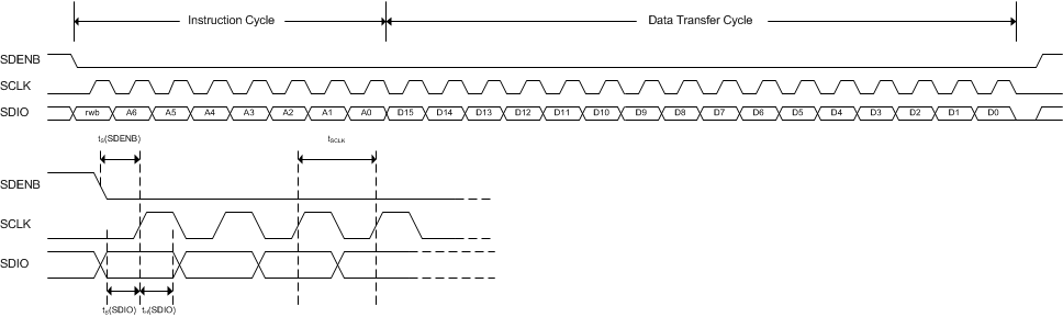 Figure 58. Serial Interface Write Timing Diagram
Figure 59 shows the serial interface timing diagram for a DAC39J82 read operation. SCLK is the serial interface clock input to the DAC39J82. Serial data enable SDENB is an active low input to the DAC39J82. SDIO is serial data in during the instruction cycle. In 3 pin configuration, SDIO is data out from the DAC39J82 during the data transfer cycle, while SDO is in a high-impedance state. In 4 pin configuration, both SDIO and SDO are data out from the DAC39J82 during the data transfer cycle. At the end of the data transfer, SDIO and SDO will output low on the final falling edge of SCLK until the rising edge of SDENB when they will 3-state.
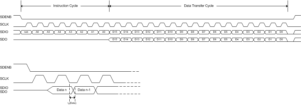 Figure 59. Serial Interface Read Timing Diagram
In the SIF interface there are four types of registers:
-
NORMAL: The NORMAL register type allows data to be written and read from. All 16-bits of the data are registered at the same time. There is no synchronizing with an internal clock thus all register writes are asynchronous with respect to internal clocks. There are three subtypes of NORMAL:
- AUTOSYNC: A NORMAL register that causes a sync to be generated after the write is finished. These are used when it is desirable to synchronize the block after writing the register or in the case of a single field that spans across multiple registers. For instance, the NCO requires three 16-bit register writes to set the frequency. Upon writing the last of these registers an autosync is generated to deliver the entire field to the NCO block at once, rather than in pieces after each individual register write. For a field that spans multiple registers, all non-AUTOSYNC registers for the field must be written first before the actual AUTOSYNC register.
- No RESET Value: These are NORMAL registers, but the reset value cannot be guaranteed. This could be because the register has some read_only bits or some internal logic partially controls the bit values.
- READ_ONLY: Registers that can be read from but not written to.
- WRITE_TO_CLEAR: These registers are just like NORMAL registers with one exception. They can be written and read, however, when the internal logic asynchronously sets a bit high in one of these registers, that bit stays high until it is written to ‘0’. This way interrupts will be captured and stay constant until cleared by the user. In the DAC39J82, register config100-108 are WRTE_TO_CLEAR registers.
7.3.8 Multi-Device Synchronization
In many applications, such as multi-antenna systems where the various transmit channels information is correlated, it is required that the latency across the link is deterministic and multiple DAC devices are completely synchronized such that their outputs are phase aligned. The DAC39J82 achieves the deterministic latency using SYSREF (JESD204B Subclass 1).
SYSREF is generated from the same clock domain as DACCLK, and is sampled at the rising edges of the device clock. It can be periodic, single-shot or “gapped” periodic. After having resynchronized its local multiframe clock (LMFC) to SYSREF, the DAC will request a link re-initialization via SYNC interface. Processing of the signal on the SYSREF input can be enabled and disabled via the SPI interface.
7.3.9 Input Multiplexer
The DAC39J82 includes a multiplexer after the JESD204B interface that allows any input stream A-B to be routed to any signal cannel A-B. See pathx_in_sel for details on how to configure the cross-bar switches.
7.3.10 FIR Filters
Figure 60 through Figure 63 show the magnitude spectrum response for the FIR0, FIR1, FIR2 and FIR3 interpolating filters where fIN is the input data rate to the FIR filter. Figure 64 to Figure 67 show the composite filter response for 2x, 4x, 8x and 16x interpolation. The transition band for all interpolation settings is from 0.4 to 0.6 x fDATA (the input data rate to the device) with < 0.001dB of pass-band ripple and > 90 dB stop-band attenuation.
The DAC39J82 includes a no interpolation 1x mode. However, the input data rate in this mode is limited to 1230 MSPS. See more details in Table 9.
The DAC39J82 also has a 9-tap inverse sinc filter (FIR4) that runs at the DAC update rate (fDAC) that can be used to flatten the frequency response of the sample-and-hold output. The DAC sample-and-hold output sets the output current and holds it constant for one DAC clock cycle until the next sample, resulting in the well-known sin(x)/x or sinc(x) frequency response (Figure 68, red line). The inverse sinc filter response (Figure 68, blue line) has the opposite frequency response from 0 to 0.4 x Fdac, resulting in the combined response (Figure 68, green line). Between 0 to 0.4 x fDAC, the inverse sinc filter compensates the sample-and-hold roll-off with less than 0.03 dB error.
The inverse sinc filter has a gain > 1 at all frequencies. Therefore, the signal input to FIR4 must be reduced from full scale to prevent saturation in the filter. The amount of back-off required depends on the signal frequency, and is set such that at the signal frequencies the combination of the input signal and filter response is less than 1 (0 dB). For example, if the signal input to FIR4 is at 0.25 x fDAC, the response of FIR4 is 0.9 dB, and the signal must be backed off from full scale by 0.9 dB to avoid saturation. The gain function in the QMC blocks can be used to reduce the amplitude of the input signal. The advantage of FIR4 having a positive gain at all frequencies is that the user is then able to optimize the back-off of the signal based on its frequency.
The filter taps for all digital filters are listed in Table 14. Note that the loss of signal amplitude may result in lower SNR due to decrease in signal amplitude.
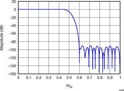
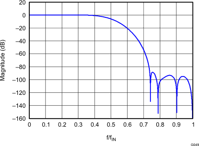
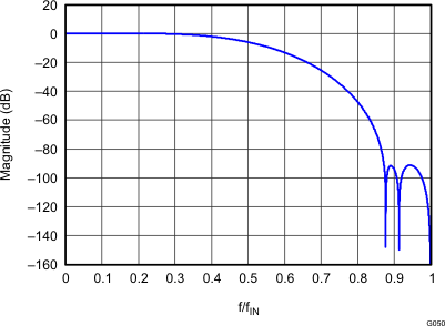
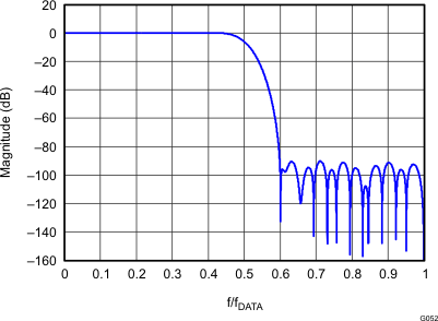
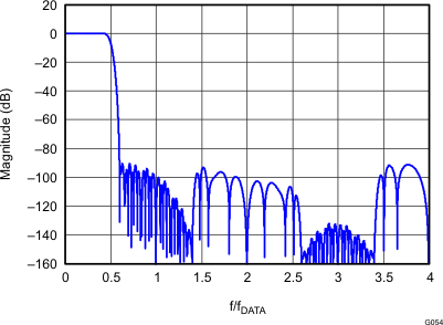
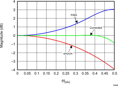
Table 11. FIR Filter Coefficients
| 2x INTERPOLATING HALF-BAND FILTERS | NON-INTERPOLATING INVERSE-SINC FILTER |
||||||||
|---|---|---|---|---|---|---|---|---|---|
| FIR0 | FIR1 | FIR2 | FIR3 | FIR4 | |||||
| 59 Taps | 23 Taps | 11 Taps | 11 Taps | 9 Taps | |||||
| 6 | 6 | –12 | –12 | 29 | 29 | 3 | 3 | 1 | 1 |
| 0 | 0 | 0 | 0 | 0 | 0 | 0 | 0 | –4 | –4 |
| –19 | –19 | 84 | 84 | –214 | –214 | –25 | –25 | 13 | 13 |
| 0 | 0 | 0 | 0 | 0 | 0 | 0 | 0 | –50 | –50 |
| 47 | 47 | –336 | –336 | 1209 | 1209 | 150 | 150 | 592(1) | |
| 0 | 0 | 0 | 0 | 2048(1) | 256(1) | ||||
| –100 | –100 | 1006 | 1006 | ||||||
| 0 | 0 | 0 | 0 | ||||||
| 192 | 192 | –2691 | –2691 | ||||||
| 0 | 0 | 0 | 0 | ||||||
| –342 | –342 | 10141 | 10141 | ||||||
| 0 | 0 | 16384(1) | |||||||
| 572 | 572 | ||||||||
| 0 | 0 | ||||||||
| –914 | –914 | ||||||||
| 0 | 0 | ||||||||
| 1409 | 1409 | ||||||||
| 0 | 0 | ||||||||
| –2119 | –2119 | ||||||||
| 0 | 0 | ||||||||
| 3152 | 3152 | ||||||||
| 0 | 0 | ||||||||
| –4729 | –4729 | ||||||||
| 0 | 0 | ||||||||
| 7420 | 7420 | ||||||||
| 0 | 0 | ||||||||
| –13334 | –13334 | ||||||||
| 0 | 0 | ||||||||
| 41527 | 41527 | ||||||||
| 65536(1) | |||||||||
7.3.11 Full Complex Mixer
The DAC39J82 has a full complex mixer (FMIX) block with a Numerically Controlled Oscillator (NCO) that enables flexible frequency placement without imposing additional limitations in the signal bandwidth. The NCO has a 48-bit frequency register (phaseaddab(47:0)) and 16-bit phase register (phaseoffsetab(15:0)) that generate the sine and cosine terms for the complex mixing. The NCO block diagram is shown in Figure 69.
 Figure 69. NCO Block Diagram
Synchronization of the NCO occurs by resetting the NCO accumulator to zero. The synchronization source is selected by syncsel_NCO(3:0) in config31. The frequency word in the phaseaddab(47:0) register is added to the accumulator every clock cycle, fDAC. The output frequency of the NCO is:
Treating the complex channel in the DAC39J82 as a complex vector of the form I + j Q, the output of FMIX IOUT(t) and QOUT(t) is
IOUT(t) = (IIN(t)cos(2πfNCOt + δ) – QIN(t)sin(2πfNCOt + δ)) x 2(mixer_gain – 1)
QOUT(t) = (IIN(t)sin(2πfNCOt + δ) + QIN(t)cos(2π fNCOt + δ)) x 2(mixer_gain – 1)
where t is the time since the last resetting of the NCO accumulator, δ is the phase offset value and mixer_gain is either 0 or 1. δ is given by:
δ = 2π × phase_offsetAB(15:0)/216
A block diagram of the mixer is shown in Figure 70. The complex mixer can be used as a digital quadrature modulator with a real output simply by only using the IOUT branch and ignoring the QOUT branch.
 Figure 70. Complex Mixer Block Diagram
The maximum output amplitude of FMIX occurs if IIN(t) and QIN(t) are simultaneously full scale amplitude and the sine and cosine arguments are equal to 2π × fNCOt + δ (2N-1) x π/4 (N = 1, 2, ...).
With mixer_gain = 0 in config2, the gain through FMIX is sqrt(2)/2 or –3 dB. This loss in signal power is in most cases undesirable, and it is recommended that the gain function of the QMC block be used to increase the signal by 3 dB to compensate. With mixer_gain = 1, the gain through FMIX is sqrt(2) or +3 dB, which can cause clipping of the signal if IIN(t) and QIN(t) are simultaneously near full scale amplitude and should therefore be used with caution.
7.3.12 Coarse Mixer
In addition to the full complex mixer the DAC39J82 also has a coarse mixer block capable of shifting the input signal spectrum by the fixed mixing frequencies ±n × fS/8. Using the coarse mixer instead of the full mixer will result in lower power consumption.
Treating the complex channel as a complex vector of the form I(t) + j Q(t), the outputs of the coarse mixer, IOUT(t) and QOUT(t) are equivalent to:
IOUT(t) = I(t)cos(2πfCMIXt) – Q(t)sin(2πfCMIXt)
QOUT(t) = I(t)sin(2πfCMIXt) + Q(t)cos(2πfCMIXt)
where fCMIX is the fixed mixing frequency selected by cmix=(fs8, fs4, fs2, fsm4). The mixing combinations are described in Table 12.
Table 12. Coarse Mixer Combinations
| cmix(3:0) | Fs/8 MIXER cmix(3) |
Fs/4 MIXER cmix(2) |
Fs/2 MIXER cmix(1) |
-Fs/4 MIXER cmix(0) |
MIXING MODE |
|---|---|---|---|---|---|
| 0000 | Disabled | Disabled | Disabled | Disabled | No mixing |
| 0001 | Disabled | Disabled | Disabled | Enabled | –Fs/4 |
| 0010 | Disabled | Disabled | Enabled | Disabled | Fs/2 |
| 0100 | Disabled | Enabled | Disabled | Disabled | +Fs/4 |
| 1000 | Enabled | Disabled | Disabled | Disabled | +Fs/8 |
| 1010 | Enabled | Disabled | Enabled | Disabled | –3Fs/8 |
| 1100 | Enabled | Enabled | Disabled | Disabled | +3Fs/8 |
| 1110 | Enabled | Enabled | Enabled | Disabled | –Fs/8 |
| All others | — | — | — | — | Not recommended |
7.3.13 Dithering
The DAC39J82 supports the addition of a band limited dither to the DAC output after the complex mixer. This feature is enabled by set dither_ena to “1” and can be useful in reducing the high order harmonics. The generated dithering sequence can be optionally up-converted to an offset of Fs/2 by setting dither_mixer_ena to “1”. The added dithering sequence has variable amplitude in 6 dB steps via dither_sra_sel.
7.3.14 Quadrature Modulation Correction (QMC)
7.3.14.1 Gain and Phase Correction
The DAC39J82 includes a Quadrature Modulator Correction (QMC) block. The QMC blocks provide a mean for changing the gain and phase of the complex signals to compensate for any I and Q imbalances present in an analog quadrature modulator. The block diagram for the QMC block is shown in Figure 71. The QMC block contains 3 programmable parameters.
Registers mem_qmc_gaina(10:0) and mem_qmc_gainb(10:0) controls the I and Q path gains and is an 11-bit unsigned value with a range of 0 to 1.9990 and the default gain is 1.0000. The implied decimal point for the multiplication is between bit 9 and bit 10. The resolution allows suppression to > 65 dBc for a frequency independent IQ imbalance (the fine delay FIR block also contains gain control through the filter taps or inverse gain block that allows control with > 20 bits resolution, which can be used to improve the sideband suppression).
Register mem_qmc_phaseab(11:0) control the phase imbalance between I and Q and are a 12-bit values with a range of –0.5 to approximately 0.49975. The QMC phase term is not a direct phase rotation but a constant that is multiplied by each "Q" sample then summed into the "I" sample path. This is an approximation of a true phase rotation in order to keep the implementation simple. The resolution of the phase term allows suppression to > 80 dBc for a frequency independent IQ imbalance.
LO feed-through can be minimized by adjusting the DAC offset feature described below.
 Figure 71. QMC Block Diagram
7.3.14.2 Offset Correction
Registers mem_qmc_offseta(12:0) and mem_qmc_offsetb(12:0) can be used to independently adjust the DC offsets of each channel. The offset values are in represented in 2s-complement format with a range from –4096 to 4095. The LSB resolution of the offset allows LO suppression to better than 90 dBFS.
The offset value adds a digital offset to the digital data before digital-to-analog conversion. Since the offset is added directly to the data it may be necessary to back off the signal to prevent saturation. Both data and offset values are LSB aligned.
 Figure 72. Digital Offset Block Diagram
7.3.15 Group Delay Correction Block
A complex transmitter system typically is consisted of a DAC, reconstruction filter network, and I/Q modulator. Besides the gain and phase mismatch contribution, there could also be timing mismatch contribution from each components. For instance, the timing mismatch could come from the PCB trace length variation between the I and Q channels and the group delay variation from the reconstruction filter. This timing mismatch in the complex transmitter system creates phase mismatch that varies linearly with respect to frequency. To compensate for the I/Q imbalances due to this mismatch, the DAC39J82 has group delay correction block for each DAC channel.
The DAC39J82 incorporates a FIR filter for small fractional group delay and 2 FIR filters for large fractional group delay. The input data to this block consists of a complex data (I/Q) channel i.e. 2 buses of 16-bit data. Control bits from configuration registers select the data path for all inputs through this block. Each input can either go through the small fractional delay filter (while its conjugate part goes through the matched delay line) or bypass the small fractional delay sub-block completely (matched delay line is bypassed for the conjugate part). The input to the large fractional delay F can either come from the output of small fractional delay sub-block or the original input to the block. The large fractional delay sub-block can also be completely bypassed if desired.
The DAC39J82 also include an integer delay block following each large fractional group delay filter, which can further delay the DAC output by [0-3]×Tdac. Channel A&B share the same control signal output_delayab, and channel C&D share the same control signal output_delaycd, which means that channel A&B have the same integer delay, and channel C&D have the same integer delay.
 Figure 73. Diagram of Group Delay Correction
7.3.15.1 Fine Fractional Delay FIR Filter
The coefficients of the FIR filters for small fractional delay are programmable to user defined values which allows users to implement their own filter transfer functions. Filter designs supporting group delay variation in the range [0.002 0.198]×Tdac, where T is the time period of DAC Clock, is listed in Table 14. The bit widths of all coefficients are fixed, which puts limits on the range of values each coefficient can acquire.
Table 13. Small Fractional Delay FIR Coefficient Range
| COEFFICIENT | RANGE |
|---|---|
| C0 | [–2,1] |
| C1 | [–16,15] |
| C2 | [–128,127] |
| C3 | [–512,511] |
| C4 | [–262144,262143] |
| C5 | [–512,511] |
| C6 | [–256,255] |
| C7 | [–64,63] |
| C8 | [–16,15] |
| C9 | [–2,1] |
Table 14. Example Coefficient Sets for the Small Fractional Delay
| C0 | C1 | C2 | C3 | C4 | C5 | C6 | C7 | C8 | C9 | InvGain NUMERATOR |
DELAY [Tdac] |
|---|---|---|---|---|---|---|---|---|---|---|---|
| 1 | -12 | 64 | –273 | 195897 | 393 | -137 | 43 | -9 | 1 | 5479 | 0.002 |
| 1 | -12 | 64 | -272 | 97872 | 393 | -137 | 43 | -9 | 1 | 10963 | 0.004 |
| 1 | -12 | 64 | -271 | 65138 | 394 | -137 | 43 | -9 | 1 | 16465 | 0.006 |
| 1 | -12 | 64 | -270 | 48873 | 395 | -137 | 43 | -9 | 1 | 21936 | 0.008 |
| 1 | -12 | 64 | -270 | 39068 | 395 | -137 | 43 | -9 | 1 | 27431 | 0.01 |
| 1 | -12 | 64 | -269 | 32555 | 396 | -137 | 43 | -9 | 1 | 32904 | 0.012 |
| 1 | -12 | 63 | -269 | 27892 | 396 | -137 | 43 | -9 | 1 | 38390 | 0.014 |
| 1 | -12 | 63 | -268 | 24387 | 397 | -138 | 43 | -9 | 1 | 43889 | 0.016 |
| 1 | -12 | 63 | -267 | 21666 | 398 | -138 | 43 | -9 | 1 | 49377 | 0.018 |
| 1 | -12 | 63 | -267 | 19496 | 398 | -138 | 43 | -9 | 1 | 54850 | 0.02 |
| 1 | -12 | 63 | -266 | 17722 | 399 | -138 | 43 | -9 | 1 | 60309 | 0.022 |
| 1 | -12 | 63 | -265 | 16235 | 400 | -138 | 43 | -9 | 1 | 65797 | 0.024 |
| 1 | -12 | 63 | -265 | 14981 | 400 | -138 | 43 | -9 | 1 | 71274 | 0.026 |
| 1 | -12 | 63 | -264 | 13907 | 401 | -138 | 43 | -9 | 1 | 76734 | 0.028 |
| 1 | -12 | 63 | -263 | 12973 | 402 | -138 | 43 | -9 | 1 | 82210 | 0.03 |
| 1 | -12 | 63 | -263 | 12159 | 402 | -138 | 43 | -9 | 1 | 87674 | 0.032 |
| 1 | -12 | 63 | -262 | 11439 | 403 | -138 | 43 | -9 | 1 | 93134 | 0.034 |
| 1 | -12 | 63 | -262 | 10798 | 404 | -138 | 43 | -9 | 1 | 98608 | 0.036 |
| 1 | -12 | 62 | -261 | 10227 | 404 | -139 | 43 | -9 | 1 | 104075 | 0.038 |
| 1 | -12 | 62 | -261 | 9714 | 405 | -139 | 43 | -9 | 1 | 109510 | 0.04 |
| 1 | -12 | 62 | -260 | 9246 | 406 | -139 | 43 | -9 | 1 | 114974 | 0.042 |
| 1 | -12 | 62 | -259 | 8823 | 406 | -139 | 43 | -9 | 1 | 120415 | 0.044 |
| 1 | -12 | 62 | -259 | 8435 | 407 | -139 | 43 | -9 | 1 | 125878 | 0.046 |
| 1 | -12 | 62 | -258 | 8080 | 408 | -139 | 43 | -9 | 1 | 131312 | 0.048 |
| 1 | -12 | 62 | -257 | 7754 | 408 | -139 | 43 | -9 | 1 | 136748 | 0.05 |
| 1 | -12 | 62 | -257 | 7454 | 409 | -139 | 43 | -9 | 1 | 142161 | 0.052 |
| 1 | -12 | 62 | -256 | 7174 | 410 | -139 | 43 | -9 | 1 | 147593 | 0.054 |
| 1 | -12 | 62 | -256 | 6916 | 411 | -139 | 43 | -9 | 1 | 152998 | 0.056 |
| 1 | -12 | 62 | -255 | 6675 | 411 | -139 | 43 | -9 | 1 | 158416 | 0.058 |
| 1 | -12 | 62 | -255 | 6450 | 412 | -139 | 43 | -9 | 1 | 163830 | 0.06 |
| 1 | -12 | 61 | -254 | 6239 | 413 | -140 | 43 | -9 | 1 | 169280 | 0.062 |
| 1 | -12 | 61 | -253 | 6042 | 413 | -140 | 43 | -9 | 1 | 174677 | 0.064 |
| 1 | -12 | 61 | -253 | 5856 | 414 | -140 | 43 | -9 | 1 | 180098 | 0.066 |
| 1 | -12 | 61 | -252 | 5683 | 415 | -140 | 43 | -9 | 1 | 185416 | 0.068 |
| 1 | -12 | 61 | -252 | 5518 | 416 | -140 | 43 | -9 | 1 | 190820 | 0.07 |
| 1 | -12 | 61 | -251 | 5363 | 416 | -140 | 43 | -9 | 1 | 196189 | 0.072 |
| 1 | -12 | 61 | -251 | 5215 | 417 | -140 | 43 | -9 | 1 | 201604 | 0.074 |
| 1 | -12 | 61 | -250 | 5076 | 418 | -140 | 43 | -9 | 1 | 206927 | 0.076 |
| 1 | -12 | 61 | -249 | 4944 | 419 | -140 | 43 | -9 | 1 | 212244 | 0.078 |
| 1 | -12 | 61 | -249 | 4819 | 419 | -140 | 43 | -9 | 1 | 217621 | 0.08 |
| 1 | -12 | 61 | -248 | 4700 | 420 | -140 | 43 | -9 | 1 | 222907 | 0.082 |
| 1 | -12 | 61 | -248 | 4586 | 421 | -141 | 43 | -9 | 1 | 228310 | 0.084 |
| 1 | -12 | 60 | -247 | 4477 | 422 | -141 | 43 | -9 | 1 | 233676 | 0.086 |
| 1 | -12 | 60 | -247 | 4375 | 422 | -141 | 43 | -9 | 1 | 238981 | 0.088 |
| 1 | -12 | 60 | -246 | 4275 | 423 | -141 | 43 | -9 | 1 | 244310 | 0.09 |
| 1 | -12 | 60 | -246 | 4181 | 424 | -141 | 44 | -9 | 1 | 249533 | 0.092 |
| 1 | -12 | 60 | -245 | 4090 | 425 | -141 | 44 | -9 | 1 | 254803 | 0.094 |
| 1 | -12 | 60 | -245 | 4003 | 425 | -141 | 44 | -9 | 1 | 260175 | 0.096 |
| 1 | -12 | 60 | -244 | 3920 | 426 | -141 | 44 | -9 | 1 | 265384 | 0.098 |
| 1 | -12 | 60 | -243 | 3840 | 427 | -141 | 44 | -9 | 1 | 270600 | 0.1 |
| 1 | -12 | 60 | -243 | 3763 | 428 | -141 | 44 | -9 | 1 | 275884 | 0.102 |
| 1 | -12 | 60 | -242 | 3690 | 429 | -141 | 44 | -9 | 1 | 281011 | 0.104 |
| 1 | -12 | 60 | -242 | 3619 | 429 | -142 | 44 | -9 | 1 | 286408 | 0.106 |
| 1 | -12 | 60 | -241 | 3550 | 430 | -142 | 44 | -9 | 1 | 291619 | 0.108 |
| 1 | -12 | 60 | -241 | 3484 | 431 | -142 | 44 | -9 | 1 | 296860 | 0.11 |
| 1 | -12 | 59 | -240 | 3421 | 432 | -142 | 44 | -9 | 1 | 302037 | 0.112 |
| 1 | -12 | 59 | -240 | 3360 | 433 | -142 | 44 | -9 | 1 | 307222 | 0.114 |
| 1 | -12 | 59 | -239 | 3300 | 433 | -142 | 44 | -9 | 1 | 312498 | 0.116 |
| 1 | -12 | 59 | -239 | 3243 | 434 | -142 | 44 | -9 | 1 | 317675 | 0.118 |
| 1 | -12 | 59 | -238 | 3188 | 435 | -142 | 44 | -9 | 1 | 322736 | 0.12 |
| 1 | -12 | 59 | -238 | 3134 | 436 | -142 | 44 | -9 | 1 | 327960 | 0.122 |
| 1 | -12 | 59 | -237 | 3082 | 437 | -142 | 44 | -9 | 1 | 333046 | 0.124 |
| 1 | -12 | 59 | -237 | 3033 | 438 | -143 | 44 | -9 | 1 | 338186 | 0.126 |
| 1 | -12 | 59 | -236 | 2984 | 438 | -143 | 44 | -9 | 1 | 343378 | 0.128 |
| 1 | -11 | 59 | -236 | 2937 | 439 | -143 | 44 | -9 | 1 | 348391 | 0.13 |
| 1 | -11 | 59 | -235 | 2891 | 440 | -143 | 44 | -9 | 1 | 353437 | 0.132 |
| 1 | -11 | 59 | -235 | 2847 | 441 | -143 | 44 | -9 | 1 | 358511 | 0.134 |
| 1 | -11 | 58 | -234 | 2804 | 442 | -143 | 44 | -9 | 1 | 363611 | 0.136 |
| 1 | -11 | 58 | -234 | 2762 | 443 | -143 | 44 | -9 | 1 | 368730 | 0.138 |
| 1 | -11 | 58 | -233 | 2722 | 443 | -143 | 44 | -9 | 1 | 373735 | 0.14 |
| 1 | -11 | 58 | -233 | 2682 | 444 | -143 | 44 | -9 | 1 | 378879 | 0.142 |
| 1 | -11 | 58 | -232 | 2644 | 445 | -143 | 44 | -9 | 1 | 383753 | 0.144 |
| 1 | -11 | 58 | -232 | 2607 | 446 | -143 | 44 | -9 | 1 | 388755 | 0.146 |
| 1 | -11 | 58 | -231 | 2570 | 447 | -144 | 44 | -9 | 1 | 393889 | 0.148 |
| 1 | -11 | 58 | -231 | 2535 | 448 | -144 | 44 | -9 | 1 | 398864 | 0.15 |
| 1 | -11 | 58 | -230 | 2501 | 449 | -144 | 44 | -9 | 1 | 403662 | 0.152 |
| 1 | -11 | 58 | -230 | 2467 | 449 | -144 | 44 | -9 | 1 | 408889 | 0.154 |
| 1 | -11 | 58 | -229 | 2435 | 450 | -144 | 44 | -9 | 1 | 413614 | 0.156 |
| 1 | -11 | 58 | -229 | 2403 | 451 | -144 | 44 | -9 | 1 | 418613 | 0.158 |
| 1 | -11 | 58 | -228 | 2372 | 452 | -144 | 44 | -9 | 1 | 423400 | 0.16 |
| 1 | -11 | 57 | -228 | 2342 | 453 | -144 | 44 | -9 | 1 | 428468 | 0.162 |
| 1 | -11 | 57 | -227 | 2313 | 454 | -144 | 44 | -9 | 1 | 433135 | 0.164 |
| 1 | -11 | 57 | -227 | 2284 | 455 | -144 | 44 | -9 | 1 | 438083 | 0.166 |
| 1 | -11 | 57 | -226 | 2256 | 456 | -145 | 44 | -9 | 1 | 442963 | 0.168 |
| 1 | -11 | 57 | -226 | 2228 | 457 | -145 | 44 | -9 | 1 | 447952 | 0.17 |
| 1 | -11 | 57 | -225 | 2202 | 458 | -145 | 44 | -9 | 1 | 452483 | 0.172 |
| 1 | -11 | 57 | -225 | 2175 | 459 | -145 | 44 | -9 | 1 | 457495 | 0.174 |
| 1 | -11 | 57 | -224 | 2150 | 459 | -145 | 44 | -9 | 1 | 462222 | 0.176 |
| 1 | -11 | 57 | -224 | 2125 | 460 | -145 | 44 | -9 | 1 | 467047 | 0.178 |
| 1 | -11 | 57 | -223 | 2100 | 461 | -145 | 44 | -9 | 1 | 471767 | 0.18 |
| 1 | -11 | 57 | -223 | 2076 | 462 | -145 | 44 | -9 | 1 | 476583 | 0.182 |
| 1 | -11 | 57 | -223 | 2053 | 463 | -145 | 44 | -9 | 1 | 481283 | 0.184 |
| 1 | -11 | 57 | -222 | 2030 | 464 | -145 | 44 | -9 | 1 | 485856 | 0.186 |
| 1 | -11 | 57 | -222 | 2008 | 465 | -146 | 44 | -9 | 1 | 490741 | 0.188 |
| 1 | -11 | 56 | -221 | 1986 | 466 | -146 | 44 | -9 | 1 | 495497 | 0.19 |
| 1 | -11 | 56 | -221 | 1964 | 467 | -146 | 44 | -9 | 1 | 500346 | 0.192 |
| 1 | -11 | 56 | -220 | 1943 | 468 | -146 | 44 | -9 | 1 | 504815 | 0.194 |
| 1 | -11 | 56 | -220 | 1923 | 469 | -146 | 44 | -9 | 1 | 509365 | 0.196 |
| 1 | -11 | 56 | -219 | 1903 | 470 | -146 | 44 | -9 | 1 | 513752 | 0.198 |
7.3.15.2 Coarse Fractional Delay FIR Filter
The coefficients of FIR filters for large fractional delay can only be chosen from a predefined set of values. Each set of values produces a specific delay with a step of 1/8×Tdac. The value of coefficients as well as their resultant fractional delay is provided in Table 15.
Table 15. Available Coefficient Sets for Large Fractional Delay FIR
| lfras_coefsel_x | C0 | C1 | C2 | C3 | C4 | C5 | C6 | C7 | InvGain NUMERATOR |
DELAY [Tdac] |
|---|---|---|---|---|---|---|---|---|---|---|
| 000 | -1 | 9 | -39 | 532 | 76 | -24 | 7 | -1 | 7503 | 0.1250 |
| 001 | -1 | 8 | -35 | 259 | 87 | -25 | 7 | -1 | 14028 | 0.2500 |
| 010 | -1 | 7 | -31 | 168 | 101 | -26 | 7 | -1 | 18725 | 0.3750 |
| 011 | -1 | 7 | -27 | 122 | 122 | -27 | 7 | -1 | 20764 | 0.5000 |
| 100 | — | — | — | — | — | — | — | — | — | — |
| 101 | -1 | 7 | -26 | 101 | 168 | -31 | 7 | -1 | 18725 | 06250 |
| 110 | -1 | 7 | -25 | 87 | 259 | -35 | 8 | -1 | 14028 | 0.7500 |
| 111 | -1 | 7 | -24 | 76 | 532 | -39 | 9 | -1 | 7503 | 0.8750 |
7.3.16 Output Multiplexer
The DAC39J82 provides four analog outputs and includes an output multiplexer before the digital to analog converters that allows any signal channel to be routed to any analog outputs. See pathx_out_sel for details on how to configure the cross-bar switches.
7.3.17 Power Measurement And Power Amplifier Protection
The DAC39J82 provides an optional mechanism to protect the Power Amplifier (PA) in cases when the signal power shows some abnormality. For example, if the data clock is lost, the FIFO would automatically generate a single tone signal, which causes abnormally high average power and could be dangerous to the PA. In the PA protection mechanism, the signal power is monitored by maintaining an sliding window accumulation of last N samples. N is selectable to be 64 or 128 based on the setting of pap_dlylen_sel. The average amplitude of input signal is computed by dividing accumulated value by the number of samples in the delay-line (N). The result is then compared against a threshold (pap_vth). If the threshold is violated, the delayed input signal is divided by a value chosen by pap_gain, to form a scaled down version of the input signal. Since PAP output derives from a delay-line, there is deterministic latency of at least N cycles from the block input to block output. The PA protection is enabled by setting the pap_ena bit to “1”.
 Figure 74. Diagram of Power Measurement and PA Protection Mechanism
7.3.18 Serdes Test Modes
The DAC39J82 supports a number of basic pattern generation and verification of SerDes via SIF. Three pseudo random bit stream (PRBS) sequences are available, along with an alternating 0/1 pattern and a 20-bit user-defined sequence. The 27-1,231-1 or 223-1 sequences implemented can often be found programmed into standard test equipment, such as a Bit Error Rate Tester (BERT). Pattern generation and verification selection is via the TESTPATT fields of rw_cfgrx0[14:12], as shown in Table 16.
Table 16. SerDes Test Pattern Selection
| TESTPATT | EFFECT |
|---|---|
| 000 | Test mode disabled. |
| 001 | Alternating 0/1 Pattern. An alternating 0/1 pattern with a period of 2UI. |
| 010 | Generate or Verify 27-1 PRBS. Uses a 7-bit LFSR with feedback polynomial x7 + x6 + 1. |
| 011 | Generate or Verify 223 -1 PRBS. Uses an ITU O.150 conformant 23-bit LFSR with feedback polynomial x23 + x18 + 1. |
| 100 | Generate or Verify 231-1 PRBS. Uses an ITU O.150 conformant 31-bit LFSR with feedback polynomial x31 + x28 + 1. |
| 101 | User-defined 20-bit pattern. Uses the USR PATT IEEE1500 Tuning instruction field to specify the pattern. The default value is 0x66666. |
| 11x | Reserved |
Pattern verification compares the output of the serial to parallel converter with an expected pattern. When there is a mismatch, the TESTFAIL bit is driven high, which can be programmed to come out the ALARM pin by setting dtest[3:0] to “0011”.
The DAC39J82 also provide a number of advanced diagnostic capabilities controlled by the IEEE 1500 interface. These are:
- Accumulation of pattern verification errors;
- The ability to map out the width and height of the receive eye, known as Eye Scan;
- Real-time monitoring of internal voltages and currents;
The SerDes blocks support the following IEEE1500 instructions:
Table 17. IEEE1500 Instruction for SerDes Receivers
| INSTRUCTION | OPCODE | DESCRIPTION |
|---|---|---|
| ws_bypass | 0x00 | Bypass. Selects a 1-bit bypass data register. Use when accessing other macros on the same IEEE1500 scan chain. |
| ws_cfg | 0x35 | Configuration. Write protection options for other instructions. |
| ws_core | 0x30 | Core. Fields also accessible via dedicated core-side ports. |
| ws_tuning | 0x31 | Tuning. Fields for fine tuning macro performance. |
| ws_debug | 0x32 | Debug. Fields for advanced control, manufacturing test, silicon characterization and debug |
| ws_unshadowed | 0x34 | Unshadowed. Fields for silicon characterization. |
| ws_char | 0x33 | Char. Fields used for eye scan. |
The data for each SerDes instruction is formed by chaining together sub-components called head, body (receiver or transmitter) and tail. The DAC39J82 uses two SerDes receiver blocks R0 and R1, each of which contains 4 receive lanes (channels), the data for each IEEE1500 instruction is formed by chaining {head, receive lane 0, receive lane 1, receive lane 2, receive lane 3, tail}. A description of bits in head, body and tail for each instruction is given as follows:
NOTE
All multi-bit signals in each chain are packed with bits reversed e.g. mpy[7:0] in ws_core head subchain is packed as {retime, enpll, mpy[0:7], vrange,lb[0:1]}. All DATA REGISTER READS from SerDes Block R0 should read 1 bit more than the desired number of bits and discard the first bit received on TDO e.g., to read 40-bit data from R0 block, 41 bits should be read off from TDO and the first bit received should be discarded. Similarly, any data written to SerDes Block R0 Data Registers should be prefixed with an extra 0.
Table 18. ws_cfg Chain
| FIELD | DESCRIPTION |
|---|---|
| HEAD (STARTING FROM THE MSB OF CHAIN) | |
| RETIME | No function. |
| CORE_WE | Core chain write enable. |
| RECEIVER (FOR EACH LANE 0,1,2,3) | |
| CORE_WE | Core chain write enable. |
| TUNING_WE | Tuning chain write enable. |
| DEBUG_WE | Reserved. |
| CHAR_WE | Char chain write enable. |
| UNSHADOWED_WE | Reserved. |
| TAIL (ENDING WITH THE LSB OF CHAIN) | |
| CORE_WE | Core chain write enable. |
| TUNING_WE | Tuning chain write enable. |
| DEBUG_WE | Reserved. |
| RETIME | No function. |
| CHAIN LENGTH = 26 BITS | |
Table 19. ws_core Chain
| FIELD | DESCRIPTION |
|---|---|
| HEAD (STARTING FROM THE MSB OF CHAIN) | |
| RETIME | No function. |
| ENPLL | PLL enable. |
| MPY[7:0] | PLL multiply. |
| VRANGE | VCO range. |
| ENDIVCLK | Enable DIVCLK output |
| LB[1:0] | Loop bandwidth |
| RECEIVER (FOR EACH LANE 0,1,2,3) | |
| ENRX | Receiver enable. |
| SLEEPRX | Receiver sleep mode. |
| BUSWIDTH[2:0] | Bus width. |
| RATE[1:0] | Operating rate. |
| INVPAIR | Invert polarity. |
| TERM[2:0] | Termination. |
| ALIGN[1:0] | Symbol alignment. |
| LOS[2:0] | Loss of signal enable. |
| CDR[2:0] | Clock/data recovery. |
| EQ[2:0] | Equalizer. |
| EQHLD | Equalizer hold. |
| ENOC | Offset compensation. |
| LOOPBACK[1:0] | Loopback. |
| BSINRXP | Boundary scan initialization. |
| BSINRXN | Boundary scan initialization. |
| RESERVED | Reserved. |
| testpatt[2:0] | Testpattern selection. |
| TESTFAIL | Test failure (real time). |
| LOSDTCT | Loss of signal detected (real time). |
| BSRXP | Boundary scan data. |
| BSRXN | Boundary scan data. |
| OCIP | Offset compensation in progress. |
| EQOVER | Received signal over equalized. |
| EQUNDER | Received signal under equalized. |
| LOSDTCT | Loss of signal detected (sticky). |
| SYNC | Re-alignment done, or aligned comma output (sticky) |
| RETIME | No function. |
| TAIL (ENDING WITH THE LSB OF CHAIN) | |
| CLKBYP[1:0] | Clock bypass. |
| SLEEPPLL | PLL sleep mode. |
| RESERVED | Reserved. |
| LOCK | PLL lock (real time). |
| BSINITCLK | Boundary scan initialization clock. |
| ENBSTX | Enable Tx boundary scan. |
| ENBSRX | Enable Rx boundary scan. |
| ENBSPT | Rx pulse boundary scan. |
| RESERVED | Reserved. |
| NEARLOCK | PLL near to lock. |
| UNLOCK | PLL lock (sticky). |
| CFG OVR | Configuration over-ride. |
| RETIME | No function. |
| CHAIN LENGTH = 196 BITS | |
Table 20. ws_tuning Chain
| FIELD | DESCRIPTION |
|---|---|
| HEAD (STARTING FROM THE MSB OF CHAIN) | |
| RETIME | No function. |
| RECEIVER (FOR EACH LANE 0,1,2,3) | |
| PATTERRTHR[2:0] | Resync error threshold. |
| PATT TIMER | PRBS Timer. |
| RXDSEL[3:0] | Status select. |
| ENCOR | Enable clear-on-read for error counter. |
| EQZERO[4:0] | EQZ OVRi Equalizer zero. |
| EQZ OVR | Equalizer zero over-ride. |
| EQLEVEL[15:0] | EQ OVRi Equalizer gain observe or set. |
| EQ OVR | Equalizer over-ride. |
| EQBOOST[1:0] | Equalizer gain boost. |
| RXASEL[2:0] | Selects amux output. |
| TAIL (ENDING WITH THE LSB OF CHAIN) | |
| ASEL[3:0] | Selects amux output. |
| USR PATT[19:0] | User-defined test pattern. |
| RETIME | No function. |
| CHAIN LENGTH = 174 BITS | |
Table 21. ws_char Chain
| FIELD | DESCRIPTION |
|---|---|
| HEAD (STARTING FROM THE MSB OF CHAIN) | |
| RETIME | No function. |
| RECEIVER (FOR EACH LANE 0,1,2,3) | |
| TESTFAIL | Test failure (sticky). |
| ECOUNT[11:0] | Error counter. |
| ESWORD[7:0] | Eye scan word masking. |
| ES[3:0] | Eye scan. |
| ESPO[6:0] | Eye scan phase offset. |
| ES BIT SELECT[4:0] | Eye scan compare bit select. |
| ESVO[5:0] | Eye scan voltage offset. |
| ESVO OVR | Eye scan voltage offset override. |
| ESLEN[1:0] | Eye scan run length. |
| ESRUN | Eye scan run. |
| ESDONE | Eye scan done. |
| TAIL (ENDING WITH THE LSB OF CHAIN) | |
| RETIME | No function. |
| CHAIN LENGTH = 194 BITS | |
7.3.19 Error Counter
All receive channels include a 12-bit counter for accumulating pattern verification errors. This counter is accessible via the ECOUNT IEEE1500 Char field. It is an essential part of the eye scan capability (see next section), though can be used independently of this..
The counter increments once for every cycle that the TESTFAIL bit is detected. The counter will not increment when at its maximum value (i.e., all 1s). When an IEEE1500 capture is performed, the count value is loaded into the ECOUNT scan elements (so that it can be scanned out), and the counter is then reset, provided ENCOR is set high.
ECOUNT can be used to get a measure of the bit error rate. However, as the error rate increases, it will become less accurate due to limitations of the pattern verification capabilities. Specifically, the pattern verifier checks multiple bits in parallel (as determined by the Rx bus width), and it is not possible to distinguish between 1 or more errors in this.
7.3.20 Eye Scan
All receive channels provide features which facilitate mapping the received data eye or extracting a symbol response. A number of fields accessible via the IEEE1500 Char scan chain allow the required low level data to be gathered. The process of transforming this data into a map of the eye or a symbol response must then be performed externally, typically in software.
The basic principle used is as follows:
- Enable dedicated eye scan input samplers, and generate an error when the value sampled differs from the normal data sample;
- Apply a voltage offset to the dedicated eye scan input samplers, to effectively reduce their sensitivity;
- Apply a phase offset to adjust the point in the eye that the dedicated eye scan data samples are taken;
- Reset the error counter to remove any false errors accumulated as a result of the voltage or phase offset adjustments;
- Run in this state for a period of time, periodically checking to see if any errors have occurred;
- Change voltage and/or phase offset, and repeat.
Alternatively, the algorithm can be configured to optimize the voltage offset at a specified phase offset, over a specified time interval.
Eye scan can be used in both synchronous and asynchronous systems, while receiving normal data traffic. The IEEE1500 Char fields used to directly control eye scan and symbol response extraction are ES, ESWORD, ES BIT SELECT, ESLEN, ESPO, ESVO, ESVO OVR, ESRUN and ESDONE, see Table 21. Eye scan errors are accumulated in ECOUNT.
The required eyescan mode is selected via the ES field, as shown in Table 22. When enabled, only data from the bit position within the 20-bit word specified via ES BIT SELECT is analyzed. In other words, only eye scan errors associated with data output at this bit position will accumulate in ECOUNT. The maximum legal ES BIT SELECT is 10011.
Table 22. Eye Scan Mode Selection
| ES[3:0] | EFFECT |
|---|---|
| 0000 | Disabled. Eye scan is disabled. |
| 0x01 | Compare. Counts mismatches between the normal sample and the eye scan sample if ES[2] = 0, and matches otherwise. |
| 0x10 | Compare zeros. As ES = 0x01, but only analyses zeros, and ignores ones. |
| 0x11 | Compare ones. As ES = 0x01, but only analyses ones, and ignores zeroes |
| 0100 | Count ones. Increments ECOUNT when the eye scan sample is a 1. |
| 1x00 | Average. Adjusts ESVO to the average eye opening over the time interval specified by ESLEN. Analyses zeroes when ES[2] = 0, and ones when ES[2]= 1. |
| 1001 1110 |
Outer. Adjusts ESVO to the outer eye opening (i.e. lowest voltage zero, highest voltage 1) over the time interval specified by ESLEN. 1001 analyses zeroes, 1110 analyses ones. |
| 1010 1101 |
Inner. Adjusts ESVO to the inner eye opening (i.e. highest voltage zero, lowest voltage 1) over the time interval specified by ESLEN. 1010 analyses zeroes, 1101 analyses ones. |
| 1x11 | Timed Compare. As ES = 001x, but analyses over the time interval specified by ESLEN. Analyses zeroes when ES[2] = 0, and ones when ES[2] = 1. |
When ES[3] = 0, the selected analysis runs continuously. However, when ES[3] = 1, only the number of qualified samples specified by ESLEN, as shown in Table 23. In this case, analysis is started by writing a 1 to ESRUN (it is not necessary to set it back to 0). When analysis completes, ESDONE will be set to 1.
Table 23. Eye Scan Run Length
| ESLen | NUMBER OF SAMPLES ANALYZED |
|---|---|
| 00 | 127 |
| 01 | 1023 |
| 10 | 8095 |
| 11 | 65535 |
When ESVO OVR = 1, the ESVO field determines the amount of offset voltage that is applied to the eye scan data samplers associated with rxpi and rxni. The amount of offset is variable between 0 and 300 mV in increments of ~10 mV, as shown in Table 24. When ES[3] = 1, ESVO OVR must be 0 to allow the optimized voltage offset to be read back via ESVO.
Table 24. Eye Scan Voltage Offset
| ESVO | OFFSET (mV) |
|---|---|
| 100000 | –310 |
| .. | .. |
| 111110 | –20 |
| 111111 | –10 |
| 000000 | 0 |
| 000001 | 10 |
| 000010 | 20 |
| .. | .. |
| 011111 | 300 |
The phase position of the samplers associated with rxpi and rxni, is controlled to a precision of 1/32UI. When ES is not 00, the phase position can be adjusted forwards or backwards by more than one UI using the ESPO field, as shown in Table 25. In normal use, the range should be limited to ±0.5UI (+15 to –16 phase steps).
Table 25. Eye Scan Phase Offset
| ESPO | OFFSET (1/32UI) |
|---|---|
| 011111 | +63 |
| .. | .. |
| 000001 | +1 |
| 000000 | 0 |
| 111111 | –1 |
| .. | .. |
| 100000 | –64 |
7.3.21 JESD204B Pattern Test
The DAC39J82 supports the following test patterns for JESD204B:
- Link layer test pattern
- Verify repeating /D.21.5/ high frequency pattern for random jitter (RJ)
- Verify repeating /K.28.5/ mixed frequency pattern for deterministic jitter (DJ)
- Verify repeating initial lane alignment (ILA) sequence
- RPAT, JSPAT or JTSPAT pattern can be verified using errors counter of 8b/10b errors produced over an amount of time to get an estimate of BER.
- Transport layer test pattern: implements a short transport layer pattern check based on F = 1,2,4 or 8. The short test pattern has a duration of one frame period and is repeated continuously for the duration of the test. Refer to JESD204B standard section 5.1.6 for more details.
- F = 1 : Looks for a constant 0xF1.
- F = 2 : Each frame should consist of 0xF1, 0xE2
- F = 4 : Looks for a constant 0xF1, 0xE2, 0xD3, 0xC4
- F = 8 : Each frame should consist of 0xF1, 0xE2, 0xD3, 0xC4, 0xB5, 0xA6, 0x97, 0x80
Users can select to output the internal data (ex, the 8b/10 decoder output, comma alignment output, lane alignment output, frame alignment output, descrambler output, etc ) of a JESD link for test purpose. See jesd_testbus_sel for configuration details.
7.3.22 Temperature Sensor
The DAC39J82 incorporates a temperature sensor block which monitors the temperature by measuring the voltage across 2 transistors. The voltage is converted to an 8-bit digital word using a successive-approximation (SAR) analog to digital conversion process. The result is scaled, limited and formatted as a twos complement value representing the temperature in degrees Celsius.
The sampling is controlled by the serial interface signals SDENB and SCLK. If the temperature sensor is enabled (tsense_sleep = “0” in register config26) a conversion takes place each time the serial port is written or read. The data is only read and sent out by the digital block when the temperature sensor is read in memin_tempdata in config7. The conversion uses the first eight clocks of the serial clock as the capture and conversion clock, the data is valid on the falling eighth SCLK. The data is then clocked out of the chip on the rising edge of the ninth SCLK. No other clocks to the chip are necessary for the temperature sensor operation. As a result the temperature sensor is enabled even when the device is in sleep mode.
In order for the process described above to operate properly, the serial port read from config6 must be done with an SCLK period of at least 1 μs. If this is not satisfied the temperature sensor accuracy is greatly reduced.
7.3.23 Alarm Monitoring
The DAC39J82 includes a flexible set of alarm monitoring that can be used to alert of a possible malfunction scenario. All the alarm events can be accessed either through the SIP registers and/or through the ALARM pin. Once an alarm is set, the corresponding alarm bit in register configtbd must be reset through the serial interface to allow further testing. The set of alarms includes the following conditions:
-
JESD alarms
- multiframe alignment_error. Occurs when multiframe alignment fails.
- frame alignment error. Occurs when multiframe alignment fails.
- link configuration error. Occurs when configuration data in ILA sequence does not match programmed configuration.
- elastic buffer overflow. Occurs when bad RBD value is used causing the elastic buffer to overflow.
- elastic buffer match error. Occurs when the first non-/K/ doesn’t match the programmed character.
- code synchronization error.
- 8b/10b not-in-table decode error.
- 8b/10 disparity error.
- alarm_from_shorttest. Occurs when the JESD204B interface fails the short pattern test.
-
SerDes alarms
- memin_rw_losdct. Occurs when there are loss of signal detect from SerDes lanes.
- FIFO write error. Occurs if write request and FIFO is full.
- FIFO write full: Occurs if FIFO is full.
- FIFO read error. Occurs if read request and FIFO is empty.
- FIFO read empty: Occurs if FIFO is empty.
- alarm_rw0_pll. Occurs if the PLL in the SerDes block for RX0 through RX3 goes out of lock.
- alarm_rw1_pll. Occurs if the PLL in the SerDes block for RX4 through RX7 goes out of lock.
-
SYSREF alarm
- alarm_sysref_err. Occurs when the SYSREF is received at an unexpected time. If too many of these occur it will cause the JESD to go into synchronization mode again.
-
DAC PLL alarm
- alarm_from_pll. Occurs when the DAC PLL is out of lock. This alarm can be ignored if the DAC PLL is not being used.
-
PAP alarms
- alarm_pap. Occurs when the average power is above the threshold. While any alarm_pap is asserted the attenuation for the appropriate data path is applied.
7.3.24 LVPECL Inputs
Figure 75 shows an equivalent circuit for the DAC input clock (DACCLKP/N) and the SYSREF (SYSREFP/N).
 Figure 75. DACCLKP/N and SYSREFP/N Equivalent Input Circuit
7.3.25 CMOS Digital Inputs
Figure 76 shows a schematic of the equivalent CMOS digital inputs of the DAC39J82. SDIO, SCLK, TCLK, SLEEP, TESTMODE and TXENABLE have pull-down resistors while SDENB, RESETB, TMS, TDI and TRSTB have pull-up resistors internal to the DAC39J82. See the specification table for logic thresholds. The pull-up and pull-down circuitry is approximately equivalent to 100 kΩ.
 Figure 76. CMOS Digital Equivalent Input
7.3.26 Reference Operation
The DAC39J82 uses a bandgap reference and control amplifier for biasing the full-scale output current. The full-scale output current is set by applying an external resistor RBIAS to pin BIASJ. The bias current IBIAS through resistor RBIAS is defined by the on-chip bandgap reference voltage and control amplifier. The default full-scale output current equals 64 times this bias current and can thus be expressed as:
IOUTFS = 16 x IBIAS = 64 x VEXTIO / RBIAS
The DAC39J82 has a 4-bit coarse gain control coarse_dac(3:0) in the configtbd register. Using gain control, the IOUTFS can be expressed as:
IOUTFS = (coarse_dac + 1) /16 x IBIAS x 64 = (coarse_dac + 1) /16 x VEXTIO / RBIAS x 64
where VEXTIO is the voltage at pin EXTIO. The bandgap reference voltage delivers an accurate voltage of 0.9V. This reference is active when extref_ena = ‘0’ in configtbd. An external decoupling capacitor CEXT of 0.1 µF should be connected externally to pin EXTIO for compensation. The bandgap reference can additionally be used for external reference operation. In that case, an external buffer with high impedance input should be applied in order to limit the bandgap load current to a maximum of 100 nA. The internal reference can be disabled and overridden by an external reference by setting the extref_ena control bit. Capacitor CEXT may hence be omitted. Pin EXTIO thus serves as either input or output node.
The full-scale output current can be adjusted from 30 mA down to 10 mA by varying resistor RBIAS or changing the externally applied reference voltage.
7.3.27 Analog Outputs
The CMOS DACs consist of a segmented array of PMOS current sources, capable of sourcing a full-scale output current up to 30 mA. Differential current switches direct the current to either one of the complimentary output nodes IOUTP or IOUTN. Complimentary output currents enable differential operation, thus canceling out common mode noise sources (digital feed-through, on-chip and PCB noise), dc offsets, even order distortion components, and increasing signal output power by a factor of four.
The full-scale output current is set using external resistor RBIAS in combination with an on-chip bandgap voltage reference source (+0.9 V) and control amplifier. Current IBIAS through resistor RBIAS is mirrored internally to provide a maximum full-scale output current equal to 16 times IBIAS.
The relation between IOUTP and IOUTN can be expressed as:
IOUTFS = IOUTP + IOUTN
We will denote current flowing into a node as –current and current flowing out of a node as +current. Since the output stage is a current source the current flows from the IOUTP and IOUTN pins. The output current flow in each pin driving a resistive load can be expressed as:
IOUTP = IOUTFS x CODE / 65536
IOUTN = IOUTFS x (65535 – CODE) / 65536
where CODE is the decimal representation of the DAC data input word.
For the case where IOUTP and IOUTN drive resistor loads RL directly, this translates into single ended voltages at IOUTP and IOUTN:
VOUTP = IOUT1 x RL
VOUTN = IOUT2 x RL
Assuming that the data is full scale (65535 in offset binary notation) and the RL is 25 Ω, the differential voltage between pins IOUTP and IOUTN can be expressed as:
VOUTP = 20mA x 25 Ω = 0.5 V
VOUTN = 0mA x 25 Ω = 0 V
VDIFF = VOUTP – VOUTN = 0.5 V
Note that care should be taken not to exceed the compliance voltages at node IOUTP and IOUTN, which would lead to increased signal distortion.
7.3.28 DAC Transfer Function
The DAC39J82 can be easily configured to drive a doubly terminated 50 Ω cable using a properly selected RF transformer. Figure 77 and Figure 78 show the 50 Ω doubly terminated transformer configuration with 1:1 and 4:1 impedance ratio, respectively. Note that the center tap of the primary input of the transformer has to be grounded to enable a DC current flow. Applying a 20-mA full-scale output current would lead to a 0.5 Vpp for a 1:1 transformer and a 1-Vpp output for a 4:1 transformer. The low dc-impedance between IOUTP or IOUTN and the transformer center tap sets the center of the ac-signal to GND, so the 1-Vpp output for the 4:1 transformer results in an output between –0.5 V and +0.5 V.
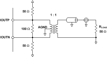 Figure 77. Driving a Doubly Terminated 50-Ω Cable Using a 1:1 Impedance Ratio Transformer
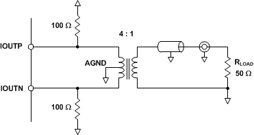 Figure 78. Driving a Doubly Terminated 50-Ω Cable Using a 4:1 Impedance Ratio Transformer
7.4 Device Functional Modes
7.4.1 Clocking Modes
The DAC39J82 has a single differential clock DACCLKN/P to clock the DAC cores and internal digital logic. The DAC39J82 DACCLK can be sourced directly or generated through an on-chip low-jitter phase-locked loop (PLL).
In those applications requiring extremely low noise it is recommended to bypass the PLL and source the DAC clock directly from a high-quality external clock to the DACCLK input. In most applications system clocking can be simplified by using the on-chip PLL to generate the DAC core clock while still satisfying performance requirements. In this case the DACCLK pins are used as the reference frequency input to the PLL.
7.4.1.1 PLL Bypass Mode
In PLL bypass mode a high quality clock is sourced to the DACCLK inputs. This clock is used to directly clock the DAC39J82 DAC cores. This mode gives the device best performance and is recommended for extremely demanding applications.
The bypass mode is selected by setting the following:
- pll_ena bit in register config49 to “0” to bypass the PLL circuitry.
- pll_sleep bit in register config26 to “1” to put the PLL and VCO into sleep mode.
7.4.1.2 PLL Mode
In this mode the clock at the DACCLK input functions as a reference clock source to the on-chip PLL. The on-chip PLL will then multiply this reference clock to supply a higher frequency DAC cores clock. Figure 79 shows the block diagram of the PLL circuit, where N divider ratio ranges from 1 to 32, M divider ratio ranges from 1 to 256, and VCO prescaler divider from 2 to 18.
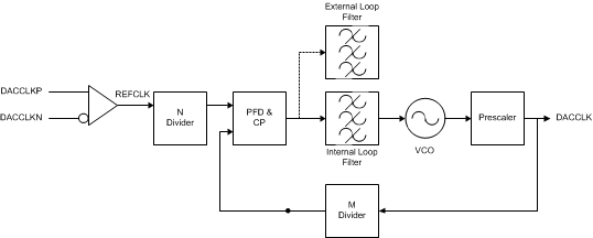 Figure 79. PLL Block Diagram
The DAC39J82 PLL mode is selected by setting the following:
- pll_ena bit in register config49 to “1” to route to the PLL and clock path.
- pll_sleep bit in register config26 to “0” to enable the PLL and VCO.
The output frequency of the VCO covers two frequency spans: H-band (4.44–5.6 GHz) and L-band (3.7–4.66 GHz). When pll_vcosel in register config51 is “1”, the L-band is selected; when pll_vcosel is “0”, the H-band is selected. At each band, the VCO range can be further adjusted by using the 6-bits pll_vco in register config51. Figure 80 shows a typical relationship between the PLL VCO coarse tuning bits pll_vco and the VCO center frequency. The corresponding equations for the H-band and L-band VCO are given in Equation 1 and Equation 2, respectively. Note that It is recommended to shift pll_vco by +1 to ensure the VCO operation at hot temp environment. In case of cold temp environment, shift by -1 on the variable pll_vco is recommended.
where pll_vcosel = "0" and pll_vcoitune = "11".
where pll_vcosel = "1" and pll_vcoitune = "10".
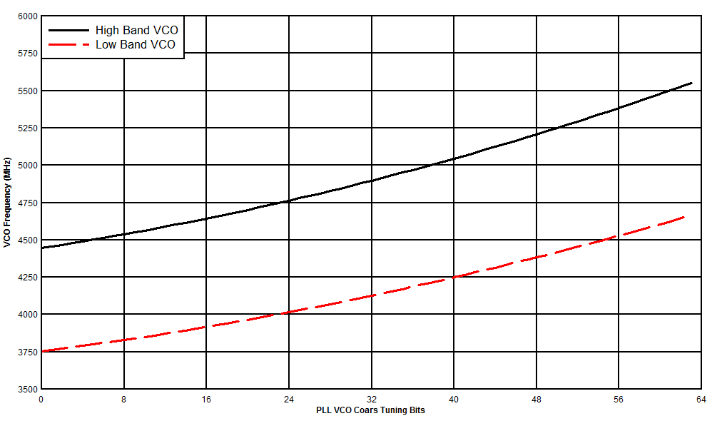 Figure 80. Typical PLL VCO Center Frequency vs Coarse Tuning Bits
Common wireless infrastructure frequencies are generated from this VCO frequency in conjunction with the pre-scaler setting pll_p in register config50 as shown in Table 26. When there are multiple valid VCO frequency and the pre-scaler settings to generate the same desired DACCLK frequency, higher pre-scaler divider ratio is recommended for better phase noise performance.
Table 26. VCO Operation
| VCO FREQUENCY (MHz) | pll_vcosel | PRE-SCALE DIVIDER | DESIRED DACCLK (MHz) | pll_p(3:0) |
|---|---|---|---|---|
| 4915.2 | 0 | 2 | 2457.6 | 0000 |
| 3932.16 | 1 | 2 | 1966.08 | 0000 |
| 4423.68 | 1 | 3 | 1474.56 | 0001 |
| 4915.2 | 0 | 4 | 1228.8 | 0010 |
| 4915.2 | 0 | 5 | 983.04 | 0011 |
| 5160.96 | 0 | 7 | 737.28 | 0101 |
| 4915.2 | 0 | 8 | 614.4 | 0110 |
| 4915.2 | 0 | 10 | 491.52 | 0111 |
The M divider is used to determine the phase-frequency-detector (PFD) and charge-pump (CP) frequency.
Table 27. PFD and CP Operation
| DACCLK FREQUENCY (MHz) | M DIVIDER | PFD UPDATE RATE (MHz) | pll_m(7:0) |
|---|---|---|---|
| 1474.56 | 12 | 122.88 | 00001011 |
| 1474.56 | 24 | 61.44 | 00010111 |
| 1474.56 | 48 | 30.72 | 00101111 |
| 1474.56 | 64 | 15.36 | 00111111 |
The N divider in the loop allows the PFD to operate at a lower frequency than the reference clock.
The overall divide ratio inside the loop is the product of the Pre-Scale and M dividers (P*M). The 5-bit pll_cp_adj is to set the charge pump current from 0 to 1.55 mA with a step of 50 µA. In nominal condition, if vco runs at 5 GHz with P-ratio and M-ratio set as 2 and 4, the DACCLK frequency would be 2.5GHz and PFD frequency 625 MHz. This needs 600µA charge pump current to stabilize the loop and gives the optimized phase noise performance. When P*M ratio increases, the charge pump current needs to be increased accordingly to sustain enough phase margin for the loop. By tuning the charge pump current, a wide range of PM ratio can be supported with the internal loop filter. In very extreme cases when the P*M ratio is huge (ex. PFD frequency of 10 MHz, VCO frequency of 4 GHz) and the loop cannot be stabilized even with the largest charge pump current, an external loop filter is required.
7.4.2 PRBS Test Mode
The DAC39J82 supports three types of PRBS sequences (27-1, 223-1, and 231-1) to verify the SerDes via SIF. To run the PRBS test on the DAC, users first need to setup the DAC for normal use, then make the following SPI writes:
- config74, set bits 4:0 to 0x1E to disable JESD clock.
- config61, set bits 14:12 to 0x2 to enable the 7-bit PRBS test pattern; or set bits 14:12 to 0x3 to enable the 23-bit PRBS test pattern; or set bits 14:12 to 0x4 to enable the 31-bit PRBS test pattern.
- config27, set bits 11:8 to 0x3 to output PRBS testfail on ALARM pin.
- config27, set bits 14:12 to the lane to be tested (0 through 7).
- config62, make sure bits 12:11 are set to 0x0 to disable character alignment.
Users should monitor the ALARM pin to see the results of the test. If the test is failing, ALARM will be high (or toggling if marginal). If the test is passing, the ALARM will be low.
7.5 Register Map
Table 28. Register Map
| Name | Address | Default | (MSB) Bit 15 |
Bit 14 | Bit 13 | Bit 12 | Bit 11 | Bit 10 | Bit 9 | Bit 8 | Bit 7 | Bit 6 | Bit 5 | Bit 4 | Bit 3 | Bit 2 | Bit 1 | (LSB) Bit 0 |
|---|---|---|---|---|---|---|---|---|---|---|---|---|---|---|---|---|---|---|
| config0 | 0x00 | 0x0218 | qmc_ offsetab _ena | reserved | qmc _corrab _ena | reserved | interp(3:0) | alarm_zeros _txenable _ena | reserved | alarm_ zeros _jesd data_ena | alarm_out _ena | alarm _out_pol | pap _ena | inv_sinc _ab _ena | reserved | |||
| config1 | 0x01 | 0x0003 | sfrac_ ena_ab | reserved | lfrac_ ena_ab | reserved | sfrac_ sel_ab | reserved | reserved | reserved | daca_ compliment | dacb_ compliment | dacc_ compliment | dacd_ compliment | reserved | reserved | reserved | reserved |
| config2 | 0x02 | 0x2002 | dac_bitwidth(1:0) | zer _invalid _data | shorttest _ena | reserved | reserved | reserved | reserved | sif4 _ena | mixer _ena | mixer _gain | nco _ena | reserved | reserved | twos | sif_reset | |
| config3 | 0x03 | 0xF380 | coarse_dac(3:0) | reserved | fif _error _zeros _data _ena | reserved | sif _txenable | |||||||||||
| config4 | 0x04 | 0x00FF | alarms_mask(15:0) | |||||||||||||||
| config5 | 0x05 | 0xFFFF | alarms_mask(31:16) | |||||||||||||||
| config6 | 0x06 | 0xFFFF | alarms_mask(47:32) | |||||||||||||||
| config7 | 0x07 | 0x0000 | memin_tempdata(7:0) | reserved | memin_lane_skew(4:0) | |||||||||||||
| config8 | 0x08 | 0x0000 | reserved | reserved | reserved | qmc_offseta(12:0) | ||||||||||||
| config9 | 0x09 | 0x0000 | reserved | reserved | reserved | qmc_offsetb(12:0) | ||||||||||||
| config10 | 0x0A | 0x0000 | reserved | reserved | reserved | reserved | ||||||||||||
| config11 | 0x0B | 0x0000 | reserved | reserved | reserved | reserved | ||||||||||||
| config12 | 0x0C | 0x0400 | reserved | reserved | reserved | reserved | reserved | qmc_gaina(10:0) | ||||||||||
| config13 | 0x0D | 0x0400 | fs8 | fs4 | fs2 | fsm4 | reserved | qmc_gainb(10:0) | ||||||||||
| config14 | 0x0E | 0x0400 | reserved | reserved | reserved | reserved | reserved | reserved | ||||||||||
| config15 | 0x0F | 0x0400 | output _delayab(1:0) | output _delaycd(1:0) | reserved | reserved | ||||||||||||
| config16 | 0x10 | 0x0000 | reserved | reserved | reserved | reserved | qmc_phaseab(11:0) | |||||||||||
| config17 | 0x11 | 0x0000 | reserved | reserved | reserved | reserved | reserved | |||||||||||
| config18 | 0x12 | 0x0000 | phaseoffsetab(15:0) | |||||||||||||||
| config19 | 0x13 | 0x0000 | reserved | |||||||||||||||
| config20 | 0x14 | 0x0000 | phaseaddab(15:0) | |||||||||||||||
| config21 | 0x15 | 0x0000 | phaseaddab(31:16) | |||||||||||||||
| config22 | 0x16 | 0x0000 | phaseaddab(47:32) | |||||||||||||||
| config23 | 0x17 | 0x0000 | reserved | |||||||||||||||
| config24 | 0x18 | 0x0000 | reserved | |||||||||||||||
| config25 | 0x19 | 0x0000 | reserved | |||||||||||||||
| config26 | 0x1A | 0x0020 | reserved | reserved | vbgr _sleep | biasopamp _sleep | tsense _sleep | pll _sleep | clkrecv _sleep | daca _sleep | dacb _sleep | dacc _sleep | dacd _sleep | |||||
| config27 | 0x1B | 0x0000 | extref _ena | dtest_lane(2:0) | dtest(3:0) | reserved | reserved | atest(5:0) | ||||||||||
| config28 | 0x1C | 0x0000 | reserved | reserved | ||||||||||||||
| config29 | 0x1D | 0x0000 | reserved | reserved | ||||||||||||||
| config30 | 0x1E | 0x1111 | syncsel_qmoffsetab(3:0) | reserved | syncsel_qmcorrab(3:0) | reserved | ||||||||||||
| config31 | 0x1F | 0x1140 | syncsel_mixerab(3:0) | reserved | syncsel_nco(3:0) | reserved | sif_sync | reserved | ||||||||||
| config32 | 0x20 | 0x0000 | syncsel_dither(3:0) | reserved | syncsel_pap(3:0) | syncsel_fir5a(3:0) | ||||||||||||
| config33 | 0x21 | 0x0000 | reserved | |||||||||||||||
| config34 | 0x22 | 0x1B1B | patha_in_sel(1:0) | pathb_in_sel(1:0) | reserved | reserved | patha_out_sel(1:0) | pathb_out_sel(1:0) | pathc_out_sel(1:0) | pathd_out_sel(1:0) | ||||||||
| config35 | 0x23 | 0xFFFF | sleep_cntl(15:0) | |||||||||||||||
| config36 | 0x24 | 0x0000 | reserved | cdrvser_sysref_mode(2:0) | reserved | reserved | ||||||||||||
| config37 | 0x25 | 0x0000 | clkjesd_div(2:0) | reserved | reserved | reserved | reserved | reserved | ||||||||||
| config38 | 0x26 | dither_ena(3:0) | dither_mixer_ena(3:0) | dither_sra_sel3:0) | reserved | reserved | dither _zero | |||||||||||
| config39 | 0x27 | 0x0000 | reserved(15:0) | |||||||||||||||
| config40 | 0x28 | 0x0000 | reserved(15:0) | |||||||||||||||
| config41 | 0x29 | 0x0000 | reserved(15:0) | |||||||||||||||
| config42 | 0x2A | 0x0000 | reserved(15:0) | |||||||||||||||
| config43 | 0x2B | 0x0000 | reserved(15:0) | |||||||||||||||
| config44 | 0x2C | 0x0000 | reserved(15:0) | |||||||||||||||
| config45 | 0x2D | 0x0000 | reserved | reserved | pap_ dlylen_sel | pap_gain(2:0) | ||||||||||||
| config46 | 0x2E | 0xFFFF | pap_vth(15:0) | |||||||||||||||
| config47 | 0x2F | 0x0004 | reserved | titest_dieid _read_ena | reserved | reserved | reserved | reserved | sifdac_ena | |||||||||
| config48 | 0x30 | 0x0000 | sifdac(15:0) | |||||||||||||||
| config49 | 0x31 | 0x0000 | lockdet_adj(2:0) | pll_reset | pll_ndivsync_ena | pll_ena | pll_cp(1:0) | pll_n(4:0) | memin_pll_lfvolt(2:0) | |||||||||
| config50 | 0x32 | 0x0000 | pll_m(7:0) | pll_p(3:0) | reserved | |||||||||||||
| config51 | 0x33 | 0x0100 | pll_vcosel | pll_vco(5:0) | pll_vcoitune(1:0) | pll_cp_adj(4:0) | reserved | |||||||||||
| config52 | 0x34 | 0x0000 | syncb _lvds _lopwrb | syncb _lvds _lopwra | syncb _lvds _lpsel | syncb _lvds _effuse _sel | reserved | reserved | lvds _sleep | lvds _sub_ena | reserved(6:0) | |||||||
| config53 | 0x35 | 0x0000 | reserved | reserved | reserved | reserved | ||||||||||||
| config54 | 0x36 | 0x0000 | reserved | |||||||||||||||
| config55 | 0x37 | 0x0000 | reserved | |||||||||||||||
| config56 | 0x38 | 0x0000 | reserved | |||||||||||||||
| config57 | 0x39 | 0x0000 | reserved | |||||||||||||||
| config58 | 0x3A | 0x0000 | reserved | |||||||||||||||
| config59 | 0x3B | 0x0000 | serdes _clk_sel | serdes_refclk_div(3:0) | reserved | reserved | ||||||||||||
| config60 | 0x3C | 0x0000 | rw_cfgpll(15:0) | |||||||||||||||
| config61 | 0x3D | 0x0000 | reserved | rw_cfgrx0(14:0) | ||||||||||||||
| config62 | 0x3E | 0x0000 | rw_cfgrx0(15:0) | |||||||||||||||
| config63 | 0x3F | 0x0000 | reserved | INVPAIR(7:0) | ||||||||||||||
| config64 | 0x40 | 0x0000 | reserved | |||||||||||||||
| config65 | 0x41 | 0x0000 | errorcnt_link0(15:0) | |||||||||||||||
| config66 | 0x42 | 0x0000 | errorcnt_link1(15:0) | |||||||||||||||
| config67 | 0x43 | 0x0000 | reserved | |||||||||||||||
| config68 | 0x44 | 0x0000 | reserved | |||||||||||||||
| config69 | 0x45 | 0x0000 | reserved | |||||||||||||||
| config70 | 0x46 | 0x0044 | lid0(4:0) | lid1(4:0) | lid2(4:0) | reserved | ||||||||||||
| config71 | 0x47 | 0x190A | lid3(4:0) | lid4(4:0) | lid5(4:0) | reserved | ||||||||||||
| config72 | 0x48 | 0x31C3 | lid6(4:0) | lid7(4:0) | reserved | subclassv(2:0) | jesdv | |||||||||||
| config73 | 0x49 | 0x0000 | link_assign(15:0) | |||||||||||||||
| config74 | 0x4A | 0x001E | lane_ena(7:0) | jesd_test _seq(1:0) | dual | init_state(3:0) | jesd _reset_n | |||||||||||
| config75 | 0x4B | 0x0000 | reserved | rbd_m1(4:0) | f_m1(7:0) | |||||||||||||
| config76 | 0x4C | 0x0000 | reserved | k_m1(4:0) | reserved | reserved | reserved | l_m1(4:0) | ||||||||||
| config77 | 0x4D | 0x0300 | m_m1(7:0) | reserved | s_m1(4:0) | |||||||||||||
| config78 | 0x4E | 0x0F0F | reserved | nprime_m1(4:0) | reserved | hd | scr | n_m1(4:0) | ||||||||||
| config79 | 0x4F | 0x1CC1 | match_data(7:0) | match _specific | match _ctrl | no_lane _sync | reserved | jesd _commaalign _ena | ||||||||||
| config80 | 0x50 | 0x0000 | adjcnt_link0(3:0) | adjdir_link0 | bid_link0(3:0) | cf_link0(4:0) | cs_link0(1:0) | |||||||||||
| config81 | 0x51 | 0x00FF | did_link0(7:0) | sync_request_ena_link0(7:0) | ||||||||||||||
| config82 | 0x52 | 0x00FF | reserved | disable _err_report _link0 | phadj _link0 | error_ena_link0(7:0) | ||||||||||||
| config83 | 0x53 | 0x0000 | adjcnt_link1(3:0) | adjdir_link1 | bid_link1(3:0) | cf_link1(4:0) | cs_link1(1:0) | |||||||||||
| config84 | 0x54 | 0x00FF | did_link1(7:0) | sync_request_ena_link1(7:0) | ||||||||||||||
| config85 | 0x55 | 0x00FF | reserved | disable _err _report _link1 | phadj _link1 | error_ena_link1(7:0) | ||||||||||||
| config86 | 0x56 | 0x0000 | reserved | reserved | reserved | reserved | reserved | |||||||||||
| config87 | 0x57 | 0x00FF | reserved | reserved | ||||||||||||||
| config88 | 0x58 | 0x00FF | reserved | reserved | reserved | reserved | ||||||||||||
| config89 | 0x59 | 0x0000 | reserved | reserved | reserved | reserved | reserved | |||||||||||
| config90 | 0x5A | 0x00FF | reserved | reserved | ||||||||||||||
| config91 | 0x5B | 0x00FF | reserved | reserved | reserved | reserved | ||||||||||||
| config92 | 0x5C | 0x1111 | reserved | reserved | reserved | reserved | err_cnt _clr_link1 | sysref_mode_link1(2:0) | err_cnt _clr_link0 | sysref_mode_link0(2:0) | ||||||||
| config93 | 0x5D | 0x0000 | reserved | |||||||||||||||
| config94 | 0x5E | 0x0000 | res1(7:0) | res2(7:0) | ||||||||||||||
| config95 | 0x60 | 0x0123 | reserved | octetpath_sel(0)(2:0) | reserved | octetpath_sel(1)(2:0) | reserved | octetpath_sel(2)(2:0) | reserved | octetpath_sel(3)(2:0) | ||||||||
| config96 | 0x61 | 0x0456 | reserved | octetpath_sel(4)(2:0) | reserved | octetpath_sel(5)(2:0) | reserved | octetpath_sel(6)(2:0) | reserved | octetpath_sel(7)(2:0) | ||||||||
| config97 | 0x62 | 0x000F | syncn_pol | reserved | syncncd_sel(3:0) | syncnab_sel(3:0) | syncn_sel(3:0) | |||||||||||
| config98 | 0x63 | 0x0000 | reserved | reserved | reserved | reserved | ||||||||||||
| config98 | 0x64 | 0x0000 | reserved | reserved | reserved | reserved | Reserved | |||||||||||
| config100 | 0x65 | 0x0000 | alarm_l_error(0)(7:0) | reserved | alarm_fifo_flags(0)(3:0) | |||||||||||||
| config101 | 0x66 | 0x0000 | alarm_l_error(1)(7:0) | reserved | alarm_fifo_flags(1)(3:0) | |||||||||||||
| config102 | 0x67 | 0x0000 | alarm_l_error(2)(7:0) | reserved | alarm_fifo_flags(2)(3:0) | |||||||||||||
| config103 | 0x68 | 0x0000 | alarm_l_error(3)(7:0) | reserved | alarm_fifo_flags(3)(3:0) | |||||||||||||
| config104 | 0x69 | 0x0000 | alarm_l_error(4)(7:0) | reserved | alarm_fifo_flags(4)(3:0) | |||||||||||||
| config105 | 0x6A | 0x0000 | alarm_l_error(5)(7:0) | reserved | alarm_fifo_flags(5)(3:0) | |||||||||||||
| config106 | 0x6B | 0x0000 | alarm_l_error(6)(7:0) | reserved | alarm_fifo_flags(6)(3:0) | |||||||||||||
| config107 | 0x6C | 0x0000 | alarm_l_error(7)(7:0) | reserved | alarm_fifo_flags(7)(3:0) | |||||||||||||
| config108 | 0x6D | 0x0000 | alarm_sysref_err(3:0) | alarm_pap(3:0) | reserved | alarm_rw0 _pll | alarm_rw1 _pll | reserved | alarm_from _pll | |||||||||
| config109 | 0x6E | 0x00xx | alarm_from_shorttest(7:0) | memin_rw_losdct(7:0) | ||||||||||||||
| config110 | 0x6F | 0x0000 | sfrac_coef0_ab(1;0) | sfrac_coef1_ab(4;0) | sfrac_coef2_ab(7;0) | Reserved | ||||||||||||
| config111 | 0x70 | 0x0000 | reserved | sfrac_coef3_ab(9;0) | ||||||||||||||
| config112 | 0x71 | 0x0000 | sfrac_coef4_ab(15;0) | |||||||||||||||
| config113 | 0x72 | 0x0000 | sfrac_coef4_ab(18:16) | reserved | sfrac_coef5_ab(9;0) | |||||||||||||
| config114 | 0x73 | 0x0000 | reserved | sfrac_coef6_ab(8;0) | ||||||||||||||
| config115 | 0x74 | 0x0000 | sfrac_coef7_ab(6;0) | sfrac_coef8_ab(4;0) | sfrac_coef9_ab(1;0) | Reserved | ||||||||||||
| config116 | 0x75 | 0x0000 | sfrac_invgain_ab(15:0) | |||||||||||||||
| config117 | 0x76 | 0x0000 | sfrac_invgain_ab(19:16) | reserved | lfras_coefsel_a(2:0) | lfras_coefsel_b(2:0) | ||||||||||||
| config118 | 0x77 | 0x0000 | reserved | reserved | reserved | Reserved | ||||||||||||
| config119 | 0x78 | 0x0000 | reserved | reserved | ||||||||||||||
| config120 | 0x79 | 0x0000 | reserved | |||||||||||||||
| config121 | 0x7A | 0x0000 | reserved | reserved | reserved | |||||||||||||
| config122 | 0x7B | 0x0000 | reserved | reserved | ||||||||||||||
| config123 | 0x7C | 0x0000 | reserved | reserved | reserved | Reserved | ||||||||||||
| config124 | 0x7D | 0x0000 | reserved | |||||||||||||||
| config125 | 0x7E | 0x0000 | reserved | reserved | reserved | reserved | ||||||||||||
| config126 | 0x7F | 0x0000 | reserved | reserved | reserved | reserved | ||||||||||||
| config127 | 0x80 | 0x0000 | memin _efc _autoload _done | memin_efc_error(4:0) | reserved | reserved | vendorid(1:0) | versionid(2:0) | ||||||||||
7.5.1 Register Descriptions
7.5.1.1 config0 Register – Address: 0x00, Default: 0x0218
| 15 | 14 | 13 | 12 | 11 | 10 | 9 | 8 |
| qmc_offsetab_ena | reserved | qmc_corrab_ena | reserved | interp | |||
| 7 | 6 | 5 | 4 | 3 | 2 | 1 | 0 |
| alarm_zeros_txenable_ena | outsum_ena | alarm_zeros_jesd_data_ena | alarm_out_ena | alarm_out_pol | pap_ena | inv_sinc_ab_ena | reserved |
Table 29. config0 Register Field Descriptions
| Register Name |
Addr (Hex) |
Bit | Name | Function | Default Value |
|---|---|---|---|---|---|
| config0 | 0x0 | 15 | qmc_offsetab_ena | Enable the offset function for the AB data path when asserted. | 0 |
| 14 | reserved | reserved | 0 | ||
| 13 | qmc_corrab_ena | Enable the Quadrature Modulator Correction (QMC) function for the AB data path when asserted. | 0 | ||
| 12 | reserved | reserved | 0 | ||
| 11:08 | interp | Determines the interpolation amount. 0000: 1x 0001: 2x 0010: 4x 0100: 8x 1000: 16x |
0010 | ||
| 7 | alarm_zeros_txenable_ena | When asserted any alarm that isn’t masked will mid-level the DAC output. | 0 | ||
| 6 | reserved | reserved | 0 | ||
| 5 | alarm_zeros_jesd_data_ena | When asserted any alarm that isn’t masked will zero the data coming out of the JESD block. | 0 | ||
| 4 | alarm_out_ena | When asserted the pin ALARM becomes an output instead of a tri-stated pin. | 1 | ||
| 3 | alarm_out_pol | This bit changes the polarity of the ALARM signal. (0=negative logic, 1=positive logic) | 1 | ||
| 2 | pap_ena | Turns on the Power Amp Protection (PAP) logic. | 0 | ||
| 1 | inv_sinc_ab_ena | Turns on the inverse sinc filter for the AB path when programmed to ‘1’. | 0 | ||
| 0 | reserved | reserved | 0 |
7.5.1.2 config1 Register – Address: 0x01, Default: 0x0003
| 15 | 14 | 13 | 12 | 11 | 10 | 9 | 8 |
| sfrac_ena_ab | reserved | lfrac_ena_ab | reserved | sfrac_sel_ab | reserved | reserved | reserved |
| 7 | 6 | 5 | 4 | 3 | 2 | 1 | 0 |
| daca_ compliment | dacb_ compliment | dacc_ compliment | dacd_ compliment | reserved | reserved | reserved | reserved |
Table 30. config1 Register Field Descriptions
| Register Name |
Addr (Hex) |
Bit | Name | Function | Default Value |
|---|---|---|---|---|---|
| config1 | 0x1 | 15 | sfrac_ena_ab | Turn on the small fractional delay filter for the AB data path. | 0 |
| 14 | reserved | reserved | 0 | ||
| 13 | lfrac_ena_ab | Turn on the large fractional delay filter for the AB data path. | 0 | ||
| 12 | reserved | reserved | 0 | ||
| 11 | sfrac_sel_ab | Select which data path is delay through the filter and which is delayed through the matched delay line. 0 : Data path B goes through filter 1 : Data path A goes through filter |
0 | ||
| 10 | reserved | reserved | 0 | ||
| 9 | reserved | Reserved | 0 | ||
| 8 | reserved | Reserved | 0 | ||
| 7 | daca_ compliment | When asserted the output to the DACA is complimented. This allows the user of the chip to effectively change the + and – designations of the IOUTA pins. | 0 | ||
| 6 | dacb_ compliment | When asserted the output to the DACB is complimented. This allows the user of the chip to effectively change the + and – designations of the IOUTB pins. | 0 | ||
| 5 | dacc_ compliment | When asserted the output to the DACC is complimented. This allows the user of the chip to effectively change the + and – designations of the IOUTC pins. | 0 | ||
| 4 | dacd_ compliment | When asserted the output to the DACD is complimented. This allows the user of the chip to effectively change the + and – designations of the IOUTD pins. | 0 | ||
| 3 | reserved | Reserved | 0 | ||
| 2 | reserved | Reserved | 0 | ||
| 1 | reserved | Reserved | 1 | ||
| 0 | reserved | Reserved | 1 |
7.5.1.3 config2 Register – Address: 0x02, Default: 0x2002
| 15 | 14 | 13 | 12 | 11 | 10 | 9 | 8 |
| dac_ bitwidth | zero_ invalid_data | shorttest_ ena | reserved | reserved | reserved | reserved | |
| 7 | 6 | 5 | 4 | 3 | 2 | 1 | 0 |
| sif4_ena | mixer_ ena | mixer_ gain | nco_ena | reserved | reserved | twos | sif_reset |
Table 31. config2 Register Field Descriptions
| Register Name |
Addr (Hex) |
Bit | Name | Function | Default Value |
|---|---|---|---|---|---|
| config2 | 0x2 | 15:14 | dac_ bitwidth | Determines the bit width of the DAC. 00 : 16 bits 01 : 14 bits 10 : 16 bits 11 : 12 bits |
00 |
| 13 | zero_ invalid_data | Zero the data from the JESD block when the link is not established. | 1 | ||
| 12 | shorttest_ ena | Turns on the short test pattern of the JESD interface. | 0 | ||
| 11 | reserved | Reserved | 0 | ||
| 10 | reserved | Reserved | 0 | ||
| 9 | reserved | Reserved | 0 | ||
| 8 | reserved | Reserved | 0 | ||
| 7 | sif4_ena | When asserted the SIF interface becomes a 4 pin interface. This bit has a lower priority than the dieid_ena bit. | 0 | ||
| 6 | mixer_ ena | When set high, the mixer block is turned on. | 0 | ||
| 5 | mixer_ gain | Add 6dB of gain to the mixer output when asserted. | 0 | ||
| 4 | nco_ena | When set high, the full NCO block is turned on. This is not necessary for the fs/2, fs/4, -fs/4 and fs/8 modes. | 0 | ||
| 3 | reserved | Reserved | 0 | ||
| 2 | reserved | Reserved | 0 | ||
| 1 | twos | When asserted, this bit tells the chip to presume that 2’s complement data is arriving at the input. Otherwise offset binary is presumed. | 1 | ||
| 0 | sif_reset | A transition from 0->1 causes a reset of the SIF registers. This bit is self clearing. This bit cannot take the place of the RESETB pin during powerup. | 0 |
7.5.1.4 config3 Register – Address: 0x03, Default: 0xF380
| 15 | 14 | 13 | 12 | 11 | 10 | 9 | 8 |
| coarse_dac | reserved | reserved | reserved | reserved | |||
| 7 | 6 | 5 | 4 | 3 | 2 | 1 | 0 |
| fifo_error_zeros_data_ena | reserved | reserved | reserved | reserved | reserved | reserved | sif_ txenable |
Table 32. config3 Register Field Descriptions
| Register Name |
Addr (Hex) |
Bit | Name | Function | Default Value |
|---|---|---|---|---|---|
| config3 | 0x3 | 15:12 | coarse_dac | Scales the output current in 16 equal steps.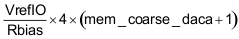 |
1111 |
| 11:8 | reserved | Reserved | 0011 | ||
| 7 | fifo_error_zeros_data_ena | When asserted SerDes FIFO errors zero the data out of the JESD block. | 1 | ||
| 6:1 | reserved | Reserved | 000000 | ||
| 0 | sif_ txenable | When asserted the internal value of TXENABLE is ‘1’. | 0 |
7.5.1.5 config4 Register – Address: 0x04, Default: 0x00FF
| 15 | 14 | 13 | 12 | 11 | 10 | 9 | 8 |
| alarms_mask(15:8) | |||||||
| 7 | 6 | 5 | 4 | 3 | 2 | 1 | 0 |
| alarms_mask(7:0) | |||||||
Table 33. config4 Register Field Descriptions
| Register Name |
Addr (Hex) |
Bit | Name | Function | Default Value |
|---|---|---|---|---|---|
| config4 | 0x4 | 15:0 | alarms_mask(15:0) | Each bit is used to mask an alarm. Assertion masks the alarm: bit15 = mask lane7 lane errors bit14 = mask lane6 lane errors bit13 = mask lane5 lane errors bit12 = mask lane4 lane errors bit11 = mask lane3 lane errors bit10 = mask lane2 lane errors bit9 = mask lane1 lane errors bit8 = mask lane0 lane errors bit7 = mask lane7 FIFO flags bit6 = mask lane6 FIFO flags bit5 = mask lane5 FIFO flags bit4 = mask lane4 FIFO flags bit3 = mask lane3 FIFO flags bit2 = mask lane2 FIFO flags bit1 = mask lane1 FIFO flags bit0 = mask lane0 FIFO flags |
0x00FF |
7.5.1.6 config5 Register – Address: 0x05, Default: 0xFFFF
| 15 | 14 | 13 | 12 | 11 | 10 | 9 | 8 |
| alarms_mask(31:24) | |||||||
| 7 | 6 | 5 | 4 | 3 | 2 | 1 | 0 |
| alarms_mask(23:16) | |||||||
Table 34. config5 Register Field Descriptions
| Register Name |
Addr (Hex) |
Bit | Name | Function | Default Value |
|---|---|---|---|---|---|
| config5 | 0x5 | 15:0 | alarms_mask(31:16) | Each bit is used to mask an alarm. Assertion masks the alarm: bit15 = always set to "1" bit14 = always set to "1" bit13 = mask SYSREF errors on link1 bit12 = mask SYSREF errors on link0 bit11 = mask alarm from PAP A block bit10 = mask alarm from PAP B block bit9 = mask alarm from PAP C block bit8 = mask alarm from PAP D block bit7 = reserved bit6 = reserved bit5 = reserved bit4 = reserved bit3 = mask alarm from SerDes block 0 PLL lock bit2 = mask alarm from SerDes block 1 PLL lock bit1 = mask SYSREF setup/hold measurement alarm bit0 = mask DAC PLL lock alarm |
0xFFFF |
7.5.1.7 config6 Register – Address: 0x06, Default: 0xFFFF
| 15 | 14 | 13 | 12 | 11 | 10 | 9 | 8 |
| alarms_mask(47:40) | |||||||
| 7 | 6 | 5 | 4 | 3 | 2 | 1 | 0 |
| alarms_mask(39:32) | |||||||
Table 35. config6 Register Field Descriptions
| Register Name |
Addr (Hex) |
Bit | Name | Function | Default Value |
|---|---|---|---|---|---|
| config6 | 0x6 | 15:0 | alarms_mask(47:32) | Each bit is used to mask an alarm. Assertion masks the alarm: bit15 = mask alarm from lane7 short test bit14 = mask alarm from lane6 short test bit13 = mask alarm from lane5 short test bit12 = mask alarm from lane4 short test bit11 = mask alarm from lane3 short test bit10 = mask alarm from lane2 short test bit9 = mask alarm from lane1 short test bit8 = mask alarm from lane0 short test bit7 = mask alarm from lane7 loss of signal detect bit6 = mask alarm from lane6 loss of signal detect bit5 = mask alarm from lane5 loss of signal detect bit4 = mask alarm from lane4 loss of signal detect bit3 = mask alarm from lane3 loss of signal detect bit2 = mask alarm from lane2 loss of signal detect bit1 = mask alarm from lane1 loss of signal detect bit0 = mask alarm from lane0 loss of signal detect |
0xFFFF |
7.5.1.8 config7 Register – Address: 0x07, Default: 0x0000
| 15 | 14 | 13 | 12 | 11 | 10 | 9 | 8 |
| memin_ tempdata | |||||||
| 7 | 6 | 5 | 4 | 3 | 2 | 1 | 0 |
| reserved | memin_lane_ skew | ||||||
Table 36. config7 Register Field Descriptions
| Register Name |
Addr (Hex) |
Bit | Name | Function | Default Value |
|---|---|---|---|---|---|
| config7 No RESET Value | 0x7 | 15:8 | memin_ tempdata | This is the output from the chip temperature sensor. NOTE: when reading these bits the SIF interface must be extremely slow, 1MHz range. | 0x00 |
| 7:5 | reserved | Reserved | 000 | ||
| 4:0 | memin_lane_ skew | Measure of the lane skew for link0 only. Updated when the RBD is released and measured in terms of JESD clock. NOTE: these bits are READ_ONLY |
0000 |
7.5.1.9 config8 Register – Address: 0x08, Default: 0x0000
| 15 | 14 | 13 | 12 | 11 | 10 | 9 | 8 |
| reserved | reserved | reserved | qmc_offseta | ||||
| 7 | 6 | 5 | 4 | 3 | 2 | 1 | 0 |
| qmc_offseta | |||||||
Table 37. config8 Register Field Descriptions
| Register Name |
Addr (Hex) |
Bit | Name | Function | Default Value |
|---|---|---|---|---|---|
| config8 AUTO SYNC | 0x8 | 15 | reserved | Reserved | 0 |
| 14 | reserved | Reserved | 0 | ||
| 13 | reserved | Reserved | 0 | ||
| 12:0 | qmc_offseta | The DAC A offset correction. The offset is measured in DAC LSBs. NOTE: Writing this register causes an auto-sync to be generated in the QMC OFFSET block. |
0x0000 |
7.5.1.10 config9 Register – Address: 0x09, Default: 0x0000
| 15 | 14 | 13 | 12 | 11 | 10 | 9 | 8 |
| reserved | reserved | reserved | qmc_offsetb | ||||
| 7 | 6 | 5 | 4 | 3 | 2 | 1 | 0 |
| qmc_offsetb | |||||||
Table 38. config9 Register Field Descriptions
| Register Name |
Addr (Hex) |
Bit | Name | Function | Default Value |
|---|---|---|---|---|---|
| config9 | 0x9 | 15:13 | reserved | Reserved | 000 |
| 12:0 | qmc_offsetb | The DAC B offset correction. The offset is measured in DAC LSBs. | 0x0000 |
7.5.1.11 config10 Register – Address: 0x0A, Default: 0x0000
| 15 | 14 | 13 | 12 | 11 | 10 | 9 | 8 |
| reserved | reserved | reserved | reserved | ||||
| 7 | 6 | 5 | 4 | 3 | 2 | 1 | 0 |
| reserved | |||||||
Table 39. config10 Register Field Descriptions
| Register Name |
Addr (Hex) |
Bit | Name | Function | Default Value |
|---|---|---|---|---|---|
| config10 AUTO SYNC |
0xA | 15:13 | reserved | reserved | 000 |
| 12:0 | reserved | reserved | 0x0000 |
7.5.1.12 config11 Register – Address: 0x0B, Default: 0x0000
| 15 | 14 | 13 | 12 | 11 | 10 | 9 | 8 |
| reserved | reserved | reserved | reserved | ||||
| 7 | 6 | 5 | 4 | 3 | 2 | 1 | 0 |
| reserved | |||||||
Table 40. config11 Register Field Descriptions
| Register Name |
Addr (Hex) |
Bit | Name | Function | Default Value |
|---|---|---|---|---|---|
| config11 | 0xB | 15:13 | reserved | reserved | 000 |
| 12:0 | reserved | reserved | 0x0000 |
7.5.1.13 config12 Register – Address: 0xC, Default: 0x0400
| 15 | 14 | 13 | 12 | 11 | 10 | 9 | 8 |
| reserved | reserved | reserved | reserved | reserved | gmc_gaina | ||
| 7 | 6 | 5 | 4 | 3 | 2 | 1 | 0 |
| gmc_gaina | |||||||
Table 41. config12 Register Field Descriptions
| Register Name |
Addr (Hex) |
Bit | Name | Function | Default Value |
|---|---|---|---|---|---|
| config12 | 0xC | 15 | reserved | Reserved | 0 |
| 14 | reserved | Reserved | 0 | ||
| 13 | reserved | Reserved | 0 | ||
| 12 | reserved | Reserved | 0 | ||
| 11 | reserved | Reserved | 0 | ||
| 10:0 | gmc_gaina | The quadrature correction gain A for DACAB path. The decimal point for the multiplication is just left of bit9. This word is treated as unsigned so the range is 0 to 1.9990. LSB=0.0009766 | 0x400 |
7.5.1.14 config13 Register – Address: 0xD, Default: 0x0400
| 15 | 14 | 13 | 12 | 11 | 10 | 9 | 8 |
| fs8 | fs4 | fs2 | fsm4 | reserved | qmc_ gainb | ||
| 7 | 6 | 5 | 4 | 3 | 2 | 1 | 0 |
| qmc_ gainb | |||||||
Table 42. config13 Register Field Descriptions
| Register Name |
Addr (Hex) |
Bit | Name | Function | Default Value |
|---|---|---|---|---|---|
| config13 | 0xD | 15 | fs8 | These bits turn on the different coarse mixing options. Combining the different options together can result in every possible n*Fs/8 [n=0->7]. Below is the valid programming table: cmix=(fs8, fs4, fs2, fsm4) 0000 : no mixing 0001 : -fs/4 0010 : fs/2 0100 : fs/4 1000 : fs/8 1100 : 3fs/8 1010 : 5fs/8 1110 : 7fs/8 |
0 |
| 14 | fs4 | 0 | |||
| 13 | fs2 | 0 | |||
| 12 | fsm4 | 0 | |||
| 11 | reserved | Reserved | 0 | ||
| 10:0 | qmc_ gainb | The quadrature correction gain B for DAC AB path. The decimal point for the multiplication is just left of bit9. This word is treated as unsigned so the range is 0 to 1.9990. LSB=0.0009766. | 0x400 |
7.5.1.15 config14 Register – Address: 0x0E, Default: 0x0400
| 15 | 14 | 13 | 12 | 11 | 10 | 9 | 8 |
| reserved | reserved | reserved | reserved | reserved | reserved | ||
| 7 | 6 | 5 | 4 | 3 | 2 | 1 | 0 |
| reserved | |||||||
Table 43. config14 Register Field Descriptions
| Register Name |
Addr (Hex) |
Bit | Name | Function | Default Value |
|---|---|---|---|---|---|
| config14 | 0xE | 15 | reserved | Reserved | 0 |
| 14 | reserved | Reserved | 0 | ||
| 13 | reserved | Reserved | 0 | ||
| 12 | reserved | Reserved | 0 | ||
| 11 | reserved | Reserved | 0 | ||
| 10:0 | reserved | Reserved | 0x400 |
7.5.1.16 config15 Register – Address: 0x0F, Default: 0x0400
| 15 | 14 | 13 | 12 | 11 | 10 | 9 | 8 |
| output _delayab | output _delaycd | reserved | reserved | ||||
| 7 | 6 | 5 | 4 | 3 | 2 | 1 | 0 |
| reserved | |||||||
Table 44. config15 Register Field Descriptions
| Register Name |
Addr (Hex) |
Bit | Name | Function | Default Value |
|---|---|---|---|---|---|
| config15 | 0xF | 15:14 | output _delayab | Delays the output to the DACs from 0 to 3 DAC clock cycles. | 00 |
| 13:12 | output _delaycd | Delays the output to the DACs from 0 to 3 DAC clock cycles. | 00 | ||
| 11 | reserved | Reserved | 0 | ||
| 10:0 | reserved | Reserved | 0x400 |
7.5.1.17 config16 Register – Address: 0x10, Default: 0x0000
| 15 | 14 | 13 | 12 | 11 | 10 | 9 | 8 |
| reserved | reserved | reserved | reserved | qmc_phaseab | |||
| 7 | 6 | 5 | 4 | 3 | 2 | 1 | 0 |
| qmc_phaseab | |||||||
Table 45. config16 Register Field Descriptions
| Register Name |
Addr (Hex) |
Bit | Name | Function | Default Value |
|---|---|---|---|---|---|
| config16 AUTO SYNC | 0x10 | 15 | reserved | Reserved | 0 |
| 14 | reserved | Reserved | 0 | ||
| 13 | reserved | Reserved | 0 | ||
| 12 | reserved | Reserved | 0 | ||
| 11:0 | qmc_phaseab | The QMC correction phase term for the DACAB path. The range is –0.5 to 0.49975. Programming “100000000000” = –0.5. Programming “011111111111” = 0.49975. | 0x000 |
7.5.1.18 config17 Register – Address: 0x11, Default: 0x0000
| 15 | 14 | 13 | 12 | 11 | 10 | 9 | 8 |
| reserved | reserved | reserved | reserved | reserved | |||
| 7 | 6 | 5 | 4 | 3 | 2 | 1 | 0 |
| reserved | |||||||
Table 46. config17 Register Field Descriptions
| Register Name |
Addr (Hex) |
Bit | Name | Function | Default Value |
|---|---|---|---|---|---|
| config17 AUTO SYNC | 0x11 | 15 | reserved | Reserved | 0 |
| 14 | reserved | Reserved | 0 | ||
| 13 | reserved | Reserved | 0 | ||
| 12 | reserved | Reserved | 0 | ||
| 11:0 | reserved | Reserved | 0x000 |
7.5.1.19 config18 Register – Address: 0x12, Default: 0x0000
| 15 | 14 | 13 | 12 | 11 | 10 | 9 | 8 |
| phaseoffsetab | |||||||
| 7 | 6 | 5 | 4 | 3 | 2 | 1 | 0 |
| phaseoffsetab | |||||||
Table 47. config18 Register Field Descriptions
| Register Name |
Addr (Hex) |
Bit | Name | Function | Default Value |
|---|---|---|---|---|---|
| config18 AUTO SYNC |
0x12 | 15:0 | phaseoffsetab | Phase offset for NCO in DACAB path | 0x0000 |
7.5.1.20 config19 Register – Address: 0x13, Default: 0x0000
| 15 | 14 | 13 | 12 | 11 | 10 | 9 | 8 |
| reserved | |||||||
| 7 | 6 | 5 | 4 | 3 | 2 | 1 | 0 |
| reserved | |||||||
Table 48. config19 Register Field Descriptions
| Register Name |
Addr (Hex) |
Bit | Name | Function | Default Value |
|---|---|---|---|---|---|
| config19 AUTO SYNC |
0x13 | 15:0 | reserved | reserved | 0x0000 |
7.5.1.21 config20 Register – Address: 0x14, Default: 0x0000
| 15 | 14 | 13 | 12 | 11 | 10 | 9 | 8 |
| phaseaddab | |||||||
| 7 | 6 | 5 | 4 | 3 | 2 | 1 | 0 |
| phaseaddab | |||||||
Table 49. config20 Register Field Descriptions
| Register Name |
Addr (Hex) |
Bit | Name | Function | Default Value |
|---|---|---|---|---|---|
| config20 | 0x14 | 15:0 | phaseaddab | Lower 16 bits of NCO Frequency adjust word for DACAB path. | 0x0000 |
7.5.1.22 config21 Register – Address: 0x15, Default: 0x0000
| 15 | 14 | 13 | 12 | 11 | 10 | 9 | 8 |
| phaseaddab | |||||||
| 7 | 6 | 5 | 4 | 3 | 2 | 1 | 0 |
| phaseaddab | |||||||
Table 50. config21 Register Field Descriptions
| Register Name |
Addr (Hex) |
Bit | Name | Function | Default Value |
|---|---|---|---|---|---|
| config21 | 0x15 | 15:0 | phaseaddab | Middle 16 bits of NCO Frequency adjust word for DACAB path. | 0x0000 |
7.5.1.23 config22 Register – Address: 0x16, Default: 0x0000
| 15 | 14 | 13 | 12 | 11 | 10 | 9 | 8 |
| phaseaddab | |||||||
| 7 | 6 | 5 | 4 | 3 | 2 | 1 | 0 |
| phaseaddab | |||||||
Table 51. config22 Register Field Descriptions
| Register Name |
Addr (Hex) |
Bit | Name | Function | Default Value |
|---|---|---|---|---|---|
| config22 | 0x16 | 15:0 | phaseaddab | Upper 16 bits of NCO Frequency adjust word for DACAB path. | 0x0000 |
7.5.1.24 config23 Register – Address: 0x17, Default: 0x0000
| 15 | 14 | 13 | 12 | 11 | 10 | 9 | 8 |
| reserved | |||||||
| 7 | 6 | 5 | 4 | 3 | 2 | 1 | 0 |
| reserved | |||||||
Table 52. config23 Register Field Descriptions
| Register Name |
Addr (Hex) |
Bit | Name | Function | Default Value |
|---|---|---|---|---|---|
| config23 | 0x17 | 15:0 | reserved | reserved | 0x0000 |
7.5.1.25 config24 Register – Address: 0x18, Default: 0x0000
| 15 | 14 | 13 | 12 | 11 | 10 | 9 | 8 |
| reserved | |||||||
| 7 | 6 | 5 | 4 | 3 | 2 | 1 | 0 |
| reserved | |||||||
Table 53. config24 Register Field Descriptions
| Register Name |
Addr (Hex) |
Bit | Name | Function | Default Value |
|---|---|---|---|---|---|
| config24 | 0x18 | 15:0 | reserved | reserved | 0x0000 |
7.5.1.26 config25 Register – Address: 0x19, Default: 0x0000
| 15 | 14 | 13 | 12 | 11 | 10 | 9 | 8 |
| reserved | |||||||
| 7 | 6 | 5 | 4 | 3 | 2 | 1 | 0 |
| reserved | |||||||
Table 54. config25 Register Field Descriptions
| Register Name |
Addr (Hex) |
Bit | Name | Function | Default Value |
|---|---|---|---|---|---|
| config25 | 0x19 | 15:0 | reserved | reserved | 0x0000 |
7.5.1.27 config26 Register – Address: 0x1A, Default: 0x0020
| 15 | 14 | 13 | 12 | 11 | 10 | 9 | 8 |
| reserved | reserved | vbgr_ sleep | |||||
| 7 | 6 | 5 | 4 | 3 | 2 | 1 | 0 |
| biasopamp_ sleep | tsense_ sleep | pll_sleep | clkrecv_sleep | daca_sleep | dacb_sleep | dacc_sleep | dacd_sleep |
Table 55. config26 Register Field Descriptions
| Register Name |
Addr (Hex) |
Bit | Name | Function | Default Value |
|---|---|---|---|---|---|
| config26 | 0x1A | 15:10 | reserved | Reserved | 000000 |
| 9 | reserved | Reserved | 0 | ||
| 8 | vbgr_ sleep | Turns off the Bandgap over internal R bias current generator bias | 0 | ||
| 7 | biasopamp_ sleep | Turns off the bias OP amp when high. | 0 | ||
| 6 | tsense_ sleep | Turns off the temperature sensor when asserted. | 0 | ||
| 5 | pll_sleep | Puts the DAC PLL into sleep mode when asserted. | 1 FUSE controlled | ||
| 4 | clkrecv_sleep | When asserted the clock input receiver gets put into sleep mode. This also affects the SYSREF receiver as well. | 0 | ||
| 3 | daca_sleep | When asserted DACA is put into sleep mode | 0 | ||
| 2 | dacb_sleep | When asserted DACB is put into sleep mode | 0 | ||
| 1 | dacc_sleep | When asserted DACC is put into sleep mode | 0 | ||
| 0 | dacd_sleep | When asserted DACD is put into sleep mode | 0 |
7.5.1.28 config27 Register – Address: 0x1B, Default: 0x0000
| 15 | 14 | 13 | 12 | 11 | 10 | 9 | 8 |
| extref_ ena | dtest_ lane | dtest | |||||
| 7 | 6 | 5 | 4 | 3 | 2 | 1 | 0 |
| reserved | reserved | atest | |||||
Table 56. config27 Register Field Descriptions
| Register Name |
Addr (Hex) |
Bit | Name | Function | Default Value |
|---|---|---|---|---|---|
| config27 | 0x1B | 15 | extref_ ena | Allows the chip to use an external reference or the internal reference. (0=internal, 1=external) | 0 |
| 14:12 | dtest_ lane | Selects the lane to output the test signal. 0=lane0, 7=lane7 | 000 | ||
| 11:8 | dtest | Allows digital test signals to come out the ALARM pin. 0000 : Test disabled, normal ALARM pin function 0001 : SERDES Block0 PLL clock/80 0010 : SERDES Block1 PLL clock/80 0011 : TESTFAIL (lane selected by dtest_lane) 0100 : SYNC(lane selected by dtest_lane) 0101 : OCIP (lane selected by dtest_lane) 0110 : EQUNDER (lane selected by dtest_lane) 0111 : EQOVER (lane selected by dtest_lane) 1000 – 1111 : not used |
0000 | ||
| 7 | reserved | Reserved | 0 | ||
| 6 | reserved | Reserved | 0 | ||
| 5:0 | atest | Selects measurement of various internal signals at the ATEST pin. 0=off 000001 : DAC PLL VSSA (0V) 000010 : DAC PLL VDD at DACCLK receiver and ndivider (0.9V) 000011 : DAC PLL 100uA bias current measurement into 0V 000100 : DAC PLL 100uA vbias at VCO (~0.8V nmos diode) 000101 : DAC PLL VDD at prescaler and mdivider (0.9V) 000110 : DAC PLL VSSA (0V) 000111 : DAC PLL VDDA1.8 (1.8V) 001000 : DAC PLL loop filter voltage (0 to 1V, ~0.5V when locked) 001001 : DACA VDDA18 (1.8V) 001010 : DACA VDDCLK (0.9) 001011 : DACA VDDDAC (0.9) 001100 : DACA VSSA (0V) 001101 : DACA VSSESD (0V) 001110 : DACA VSSA (0V) 001111 : DACA main current source PMOS cascode bias (1.65V) 010000 : DACA output switch cascode bias (0.4V) 010001 : DACB VDDA18 (1.8V) 010010 : DACB VDDCLK (0.9) 010011 : DACB VDDDAC (0.9) 010100 : DACB VSSA (0V) 010101 : DACB VSSESD (0V) 010110 : DACB VSSA (0V) 010111 : DACB main current source PMOS cascode bias (1.65V) 011000 : DACB output switch cascode bias (0.4V) 011001 : DACC VDDA18 (1.8V) 011010 : DACC VDDCLK (0.9) 011011 : DACC VDDDAC (0.9) 011100 : DACC VSSA (0V) 011101 : DACC VSSESD (0V) 011110 : DACC VSSA (0V) 011111 : DACC main current source PMOS cascode bias (1.65V) |
000000 | ||
| config27 (continued) | 0x1B | 5:0 | atest | 100000 : DACC output switch cascode bias (0.4V) 100001 : DACD VDDA18 (1.8V) 100010 : DACD VDDCLK (0.9) 100011 : DACD VDDDAC (0.9) 100100 : DACD VSSA (0V) 100101 : DACD VSSESD (0V) 100110 : DACD VSSA (0V) 100111 : DACD main current source PMOS cascode bias (1.65V) 101000 : DACD output switch cascode bias (0.4V) 101001 : Temp Sensor VSSA (0V) 101010 : Temp Sensor amplifier output (0 to 1.8V) 101011 : Temp Sensor reference output (~0.6V, can be trimmed) 101100 : Temp Sensor comparator output (0 to 1.8V) 101101 : Temp Sensor 64uA bias voltage (~0.8V nmos diode) 101110 : BIASGEN 100uA bias measured to 0V (to be trimmed) 101111 : Temp Sensor VDD (0.9V) 110000 : Temp Sensor VDDA18 (1.8V) 110001: DAC bias current measured into 1.8V. scales with coarse DAC setting (7.3µA to 117µA) 110010: Bangap PTAT current measured into 0V (~20µA) 110011: CoarseDAC PMOS current source gate (~1V) 110100: RBIAS (0.9V) 110101: EXTIO (0.9V) 110110: Bandgap PMOS cascode gate (0.7V) 110111: Bandgap startup circuit output (~0V when BG started) 111000: Bandgap output (0.9V, can be trimmed) 111001: SYNCB LVDS buffer reference voltage (1.2V) must set syncb_lvds_efuse_sel to measure. 111010: VSS in digital core MET1 (0V) 111011: VSS in digital core MET1 (0V) 111100: VSS near bump (0V) 111101: VDDDIG in digital core MET1 (0.9V) 111110: VDDDIG in digital core MET1 (0.9V) |
000000 |
7.5.1.29 config28 Register – Address: 0x1C, Default: 0x0000
| 15 | 14 | 13 | 12 | 11 | 10 | 9 | 8 |
| reserved | |||||||
| 7 | 6 | 5 | 4 | 3 | 2 | 1 | 0 |
| reserved | |||||||
Table 57. config28 Register Field Descriptions
| Register Name |
Addr (Hex) |
Bit | Name | Function | Default Value |
|---|---|---|---|---|---|
| config28 | 0x1C | 15:8 | reserved | reserved | 0x00 |
| 7:0 | reserved | reserved | 0x00 |
7.5.1.30 config29 Register – Address: 0x1D, Default: 0x0000
| 15 | 14 | 13 | 12 | 11 | 10 | 9 | 8 |
| reserved | |||||||
| 7 | 6 | 5 | 4 | 3 | 2 | 1 | 0 |
| reserved | |||||||
Table 58. config29 Register Field Descriptions
| Register Name |
Addr (Hex) |
Bit | Name | Function | Default Value |
|---|---|---|---|---|---|
| config29 | 0x1D | 15:8 | reserved | reserved | 0x00 |
| 7:0 | reserved | reserved | 0x00 |
7.5.1.31 config30 Register – Address: 0x1E, Default: 0x1111
| 15 | 14 | 13 | 12 | 11 | 10 | 9 | 8 |
| syncsel_ qmoffsetab | reserved | ||||||
| 7 | 6 | 5 | 4 | 3 | 2 | 1 | 0 |
| syncsel_ qmcorrab | reserved | ||||||
Table 59. config30 Register Field Descriptions
| Register Name |
Addr (Hex) |
Bit | Name | Function | Default Value |
|---|---|---|---|---|---|
| config30 | 0x1E | 15:12 | syncsel_ qmoffsetab | Select the sync for the QMCoffsetAB block. A ‘1’ in the selected bit place allows the selected sync to pass to the block. bit0 = auto-sync from SIF register write bit1 = sysref bit2 = sync_out from JESD bit3 = sif_sync |
0x1 |
| 11:8 | reserved | reserved | 0x1 | ||
| 7:4 | syncsel_ qmcorrab | Select the sync for the QMCcorrAB block. A ‘1’ in the selected bit place allows the selected sync to pass to the block. bit0 = auto-sync from SIF register write bit1 = sysref bit2 = sync_out from JESD bit3 = sif_sync |
0x1 | ||
| 3:0 | reserved | reserved | 0x1 |
7.5.1.32 config31 Register – Address: 0x1F, Default: 0x1111
| 15 | 14 | 13 | 12 | 11 | 10 | 9 | 8 |
| syncsel_ mixerab | reserved | ||||||
| 7 | 6 | 5 | 4 | 3 | 2 | 1 | 0 |
| syncsel_ nco | reserved | sif_sync | reserved | ||||
Table 60. config31 Register Field Descriptions
| Register Name |
Addr (Hex) |
Bit | Name | Function | Default Value |
|---|---|---|---|---|---|
| config31 | 0x1F | 15:12 | syncsel_ mixerab | Select the sync for the mixerAB block. A ‘1’ in the selected bit place allows the selected sync to pass to the block. bit0 = auto-sync from SIF register write bit1 = sysref bit2 = sync_out from JESD bit3 = sif_sync |
0x1 |
| 11:8 | reserved | Reserved | 0x1 | ||
| 7:4 | syncsel_ nco | Select the sync for the NCO accumulators. A ‘1’ in the selected bit place allows the selected sync to pass to the block. bit0 = ‘0’ bit1 = sysref bit2 = sync_out from JESD bit3 = sif_sync |
0x4 | ||
| 3:2 | reserved | Reserved | 00 | ||
| 1 | sif_sync | This is the SIF SYNC signal. | 0 | ||
| 0 | reserved | Reserved | 0 |
7.5.1.33 config32 Register – Address: 0x20, Default: 0x0000
| 15 | 14 | 13 | 12 | 11 | 10 | 9 | 8 |
| syncsel_ dither | reserved | ||||||
| 7 | 6 | 5 | 4 | 3 | 2 | 1 | 0 |
| syncsel_ pap | syncsel_ fir5a | ||||||
Table 61. config32 Register Field Descriptions
| Register Name |
Addr (Hex) |
Bit | Name | Function | Default Value |
|---|---|---|---|---|---|
| config32 | 0x20 | 15:12 | syncsel_ dither | Select the sync for the Dithering block. bit0 = ‘0’ bit1 = sysref bit2 = sync_out from JESD bit3 = sif_sync |
0x0 |
| 11:8 | reserved | Reserved | 0x0 | ||
| 7:4 | syncsel_ pap | 7:4 Select the sync for the PA Protection block. bit0 = ‘0’ bit1 = sysref bit2 = sync_out from JESD bit3 = sif_sync 0x0 |
0x0 | ||
| 3:0 | syncsel_ fir5a | Select the sync for the small fractional delay FIR filter coefficient loading. bit0 = ‘0’ bit1 = sysref bit2 = sync_out from JESD bit3 = sif_sync |
0x0 |
7.5.1.34 config33 Register – Address: 0x21, Default: 0x0000
| 15 | 14 | 13 | 12 | 11 | 10 | 9 | 8 |
| reserved | |||||||
| 7 | 6 | 5 | 4 | 3 | 2 | 1 | 0 |
| reserved | |||||||
Table 62. config33 Register Field Descriptions
| Register Name |
Addr (Hex) |
Bit | Name | Function | Default Value |
|---|---|---|---|---|---|
| config33 | 0x21 | 15:0 | reserved | Reserved | 0x0000 |
7.5.1.35 config34 Register – Address: 0x22, Default: 0x1B1B
| 15 | 14 | 13 | 12 | 11 | 10 | 9 | 8 |
| patha_in _sel | pathb_in _sel | reserved | reserved | ||||
| 7 | 6 | 5 | 4 | 3 | 2 | 1 | 0 |
| patha_ out_sel | pathb_ out_sel | pathc_ out_sel | pathd_ out_sel | ||||
Table 63. config34 Register Field Descriptions
| Register Name |
Addr (Hex) |
Bit | Name | Function | Default Value |
|---|---|---|---|---|---|
| config34 | 0x22 | 15:14 | patha_in _sel | This selects the word used for the path A input. 00 = Sample 0 from JESD is selected for data path A 01 = Sample 1 from JESD is selected for data path A 10 = Sample 2 from JESD is selected for data path A 11 = Sample 3 from JESD is selected for data path A |
00 |
| 13:12 | pathb_in _sel | This selects the word used for the path B input. 00 = Sample 0 from JESD is selected for data path B 01 = Sample 1 from JESD is selected for data path B 10 = Sample 2 from JESD is selected for data path B 11 = Sample 3 from JESD is selected for data path B |
01 | ||
| 11:10 | reserved | reserved | 10 | ||
| 9:8 | reserved | reserved | 11 | ||
| 7:6 | patha_ out_sel | This selects the word used for the DACA output. 00 = data path A goes to DACA 01 = data path B goes to DACA 10 = zeroes go to DACA 11 = zeroes go to DACA |
00 | ||
| 5:4 | pathb_ out_sel | This selects the word used for the DACB output. 00 = data path A goes to DACB 01 = data path B goes to DACB 10 = zeroes go to DACB 11 = zeroes go to DACB |
01 | ||
| 3:2 | pathc_ out_sel | This selects the word used for the DACC output. 00 = data path A goes to DACC 01 = data path B goes to DACC 10 = zeroes go to DACC 11 = zeroes go to DACC |
10 | ||
| 1:0 | pathd_ out_sel | This selects the word used for the DACD output. 00 = data path A goes to DACD 01 = data path B goes to DACD 10 = zeroes go to DACD 11 = zeroes go to DACD |
11 |
7.5.1.36 config35 Register – Address: 0x23, Default: 0xFFFF
| 15 | 14 | 13 | 12 | 11 | 10 | 9 | 8 |
| sleep_cntl | |||||||
| 7 | 6 | 5 | 4 | 3 | 2 | 1 | 0 |
| sleep_cntl | |||||||
Table 64. config35 Register Field Descriptions
| Register Name |
Addr (Hex) |
Bit | Name | Function | Default Value |
|---|---|---|---|---|---|
| config35 | 0x23 | 15:0 | sleep_cntl | This controls the routing of the SLEEP pin signal to different blocks. Assertion means that the SLEEP signal will be sent to the block. These bits do not override the SIF bits, just the SLEEP signal from the pin. When asserted, bit15 through bit9 = Not used bit8 = Allows the Band gap over R to sleep (BUG… in this PG it is hooked to bit7) bit7 = Allows the Bias OP Amp to sleep bit6 = Allows the TEMP Sensor to sleep bit5 = Allows the PLL to sleep bit4 = Allows the CLK_RECV to sleep bit3 = Allows DACD to sleep bit2 = Allows DACC to sleep bit1 = Allows DACB to sleep bit0 = Allows DACA to sleep |
0xFFFF |
7.5.1.37 config36 Register – Address: 0x24, Default: 0x0000
| 15 | 14 | 13 | 12 | 11 | 10 | 9 | 8 |
| reserved | reserved | ||||||
| 7 | 6 | 5 | 4 | 3 | 2 | 1 | 0 |
| reserved | cdrvser_ sysref_mode | reserved | reserved | ||||
Table 65. config36 Register Field Descriptions
| Register Name |
Addr (Hex) |
Bit | Name | Function | Default Value |
|---|---|---|---|---|---|
| config36 | 0x24 | 15:13 | reserved | Reserved | 000 |
| 12:7 | reserved | Reserved | 000000 | ||
| 6:4 | cdrvser_ sysref_mode | Determines how SYSREF is used to sync the clock dividers in the device. 000 = Don’t use SYSREF pulse 001 = Use all SYSREF pulses 010 = Use only the next SYSREF pulse 011 = Skip one SYSREF pulse then use only the next one 100 = Skip one SYSREF pulse then use all pulses. |
000 | ||
| 3:2 | reserved | Reserved | 00 | ||
| 1:0 | reserved | Reserved | 00 |
7.5.1.38 config37 Register – Address: 0x25, Default: 0x8000
| 15 | 14 | 13 | 12 | 11 | 10 | 9 | 8 |
| clkjesd_ div | reserved | reserved | |||||
| 7 | 6 | 5 | 4 | 3 | 2 | 1 | 0 |
| reserved | reserved | reserved | reserved | ||||
Table 66. config37 Register Field Descriptions
| Register Name |
Addr (Hex) |
Bit | Name | Function | Default Value |
|---|---|---|---|---|---|
| config37 | 0x25 | 15:13 | clkjesd_ div | This controls the amount of dividing down the DACCLK gets to generate the JESD clock. It is independent of the interpolation because of the different JESD interfaces. “000” : DACCLK “001” : div2 “010” : div4 “011” : div8 “100” : div16 “101” : div32 “110” : always 1 “111” : always 0 |
100 |
| 12:10 | reserved | Reserved | 000 | ||
| 9:7 | reserved | Reserved | 000 | ||
| 6:4 | reserved | Reserved | 000 | ||
| 3:1 | reserved | Reserved | 000 | ||
| 0 | reserved | Reserved | 0 |
7.5.1.39 config38 Register – Address: 0x26, Default: 0x0000
| 15 | 14 | 13 | 12 | 11 | 10 | 9 | 8 |
| dither_ ena | dither_ mixer_ena | ||||||
| 7 | 6 | 5 | 4 | 3 | 2 | 1 | 0 |
| dither_sra_sel | reserved | reserved | reserved | ||||
Table 67. config38 Register Field Descriptions
| Register Name |
Addr (Hex) |
Bit | Name | Function | Default Value |
|---|---|---|---|---|---|
| config38 | 0x26 | 15:12 | dither_ ena | Turns on DITHER block for each data path bit15 = reserved bit14 = reserved bit13 = data path B bit12 = data path A |
0000 |
| 11:8 | dither_ mixer_ena | Turns on the FS/2 mixer at the output of the CIC in the DITHER block. bit11 = reserved bit10 = reserved bit9 = data path B bit8 = data path A |
0000 | ||
| 7:4 | dither_sra_sel | Select the amount of dithering added to the signal. 0 is the maximum dithering. | 0000 | ||
| 3:2 | reserved | Reserved | 00 | ||
| 1 | reserved | Reserved | 0 | ||
| 0 | reserved | Reserved | 0 |
7.5.1.40 config39 Register – Address: 0x27, Default: 0x0000
| 15 | 14 | 13 | 12 | 11 | 10 | 9 | 8 |
| reserved | |||||||
| 7 | 6 | 5 | 4 | 3 | 2 | 1 | 0 |
| reserved | |||||||
Table 68. config39 Register Field Descriptions
| Register Name |
Addr (Hex) |
Bit | Name | Function | Default Value |
|---|---|---|---|---|---|
| config39 | 0x27 | 15:0 | reserved | Reserved | 0x0000 |
7.5.1.41 config40 Register – Address: 0x28, Default: 0x0000
| 15 | 14 | 13 | 12 | 11 | 10 | 9 | 8 |
| reserved | |||||||
| 7 | 6 | 5 | 4 | 3 | 2 | 1 | 0 |
| reserved | |||||||
Table 69. config40 Register Field Descriptions
| Register Name |
Addr (Hex) |
Bit | Name | Function | Default Value |
|---|---|---|---|---|---|
| config40 WRITE TO CLEAR |
0x28 | 15:0 | reserved | Reserved | 0x0000 |
7.5.1.42 config41 Register – Address: 0x29, Default: 0x0000
| 15 | 14 | 13 | 12 | 11 | 10 | 9 | 8 |
| reserved | |||||||
| 7 | 6 | 5 | 4 | 3 | 2 | 1 | 0 |
| reserved | |||||||
Table 70. config41 Register Field Descriptions
| Register Name |
Addr (Hex) |
Bit | Name | Function | Default Value |
|---|---|---|---|---|---|
| config41 | 0x29 | 15:0 | reserved | Reserved | 0xFFFF |
7.5.1.43 config42 Register – Address: 0x2A, Default: 0x0000
| 15 | 14 | 13 | 12 | 11 | 10 | 9 | 8 |
| reserved | |||||||
| 7 | 6 | 5 | 4 | 3 | 2 | 1 | 0 |
| reserved | |||||||
Table 71. config42 Register Field Descriptions
| Register Name |
Addr (Hex) |
Bit | Name | Function | Default Value |
|---|---|---|---|---|---|
| config42 | 0x2A | 15:0 | reserved | Reserved | 0000 |
7.5.1.44 config43 Register – Address: 0x2B, Default: 0x0000
| 15 | 14 | 13 | 12 | 11 | 10 | 9 | 8 |
| reserved | |||||||
| 7 | 6 | 5 | 4 | 3 | 2 | 1 | 0 |
| reserved | |||||||
Table 72. config43 Register Field Descriptions
| Register Name |
Addr (Hex) |
Bit | Name | Function | Default Value |
|---|---|---|---|---|---|
| config43 | 0x2B | 15:0 | reserved | Reserved | 0x0000 |
7.5.1.45 config44 Register – Address: 0x2C, Default: 0x0000
| 15 | 14 | 13 | 12 | 11 | 10 | 9 | 8 |
| reserved | |||||||
| 7 | 6 | 5 | 4 | 3 | 2 | 1 | 0 |
| reserved | |||||||
Table 73. config44 Register Field Descriptions
| Register Name |
Addr (Hex) |
Bit | Name | Function | Default Value |
|---|---|---|---|---|---|
| config44 | 0x2C | 15:0 | reserved | Reserved | 0000 |
7.5.1.46 config45 Register – Address: 0x2D, Default: 0x0000
| 15 | 14 | 13 | 12 | 11 | 10 | 9 | 8 |
| reserved | reserved | ||||||
| 7 | 6 | 5 | 4 | 3 | 2 | 1 | 0 |
| reserved | pap_ dlylen_sel | pap_gain | |||||
Table 74. config45 Register Field Descriptions
| Register Name |
Addr (Hex) |
Bit | Name | Function | Default Value |
|---|---|---|---|---|---|
| config45 | 0x2D | 15 | reserved | Reserved | 0 |
| 14:4 | reserved | Reserved | 00000000000 | ||
| 3 | pap_ dlylen_sel | Select the length of the PAP average: 0 : 64 samples 1 : 128 samples |
0 | ||
| 2:0 | pap_gain | The amount of attenuation to apply when the threshold for PAP is met: 000 : no attenuation 001 : divide by 2 010 : divided by 4 011 : divided by 8 100 : divided by 16 101 : no attenuation 110 : no attenuation 111 : no attenuation |
000 |
7.5.1.47 config46 Register – Address: 0x2E, Default: 0xFFFF
| 15 | 14 | 13 | 12 | 11 | 10 | 9 | 8 |
| pap_vth | |||||||
| 7 | 6 | 5 | 4 | 3 | 2 | 1 | 0 |
| pap_vth | |||||||
Table 75. config46 Register Field Descriptions
| Register Name |
Addr (Hex) |
Bit | Name | Function | Default Value |
|---|---|---|---|---|---|
| config46 | 0x2E | 15:0 | pap_vth | The threshold value for the PA protection logic. When the power measurement is greater than this activate the PA protection logic. | 0xFFFF |
7.5.1.48 config47 Register – Address: 0x2F, Default: 0x0004
| 15 | 14 | 13 | 12 | 11 | 10 | 9 | 8 |
| reserved | titest_dieid_read_ena | reserved | reserved | ||||
| 7 | 6 | 5 | 4 | 3 | 2 | 1 | 0 |
| reserved | reserved | reserved | sifdac_ena | ||||
Table 76. config47 Register Field Descriptions
| Register Name |
Addr (Hex) |
Bit | Name | Function | Default Value |
|---|---|---|---|---|---|
| config47 | 0x2F | 15 | reserved | Reserved | 0 |
| 14 | titest_dieid_read_ena | When asserted, the die ID can be read out after fuse autoload is finished on register 100-107. When de-asserted normal function of the registers is read out. | 0 | ||
| 13 | reserved | Reserved | 0 | ||
| 12:3 | reserved | Reserved | 0000000000 | ||
| 2 | reserved | Reserved | 1 | ||
| 1 | reserved | Reserved | 0 | ||
| 0 | sifdac_ena | When asserted the DAC output is set to the value in register sifdac. | 0 |
7.5.1.49 config48 Register – Address: 0x30, Default: 0x0000
| 15 | 14 | 13 | 12 | 11 | 10 | 9 | 8 |
| sifdc | |||||||
| 7 | 6 | 5 | 4 | 3 | 2 | 1 | 0 |
| sifdc | |||||||
Table 77. config48 Register Field Descriptions
| Register Name |
Addr (Hex) |
Bit | Name | Function | Default Value |
|---|---|---|---|---|---|
| config48 | 0x30 | 15:0 | sifdc | This is the value that is sent to the digital blocks when register sifdac_ena is asserted. | 0x0000 |
7.5.1.50 config49 Register – Address: 0x31, Default: 0x0000
| 15 | 14 | 13 | 12 | 11 | 10 | 9 | 8 |
| lockdet_ adj | pll_reset | pll_ ndivsync_ena | pll_ena | pll_cp | |||
| 7 | 6 | 5 | 4 | 3 | 2 | 1 | 0 |
| pll_n | memin_pll_lfvolt | ||||||
Table 78. config49 Register Field Descriptions
| Register Name |
Addr (Hex) |
Bit | Name | Function | Default Value |
|---|---|---|---|---|---|
| config49 | 0x31 | 15:13 | lockdet_ adj | Adjusts the sensitivity of the DAC PLL lock detector; 4 settings from 000 to 011. The 011 setting has the widest lock detection window, tolerating more jitter while reporting a lock. The 000 setting has a narrow window and will indicate an unlocked state more often. | 000 |
| 12 | pll_reset | When set, the M divider, N divider and PFD are held reset. | 0 | ||
| 11 | pll_ ndivsync_ena | When on, the SYSREF input is used to sync the N dividers of the PLL. | 0 | ||
| 10 | pll_ena | Enables the PLL output as the DAC clock when set; the clock provided at the DACCLKP/N is used as the PLL reference clock. When cleared, the PLL is bypassed and the clock provided at the DACCLKP/N pins is used as the DAC clock | 0 FUSE controlled |
||
| 9:8 | pll_cp | Must be set to 00 for proper PLL operation | 00 | ||
| 7:3 | pll_n | Reference clock divider; divide by is N+1 | 00000 | ||
| 2:0 | memin_pll_lfvolt | Indicates the loop filter voltage; 111 is max, 000 is min. When the PLL is correctly programmed, this will read 011 or 100 for a centered loop filter voltage. | 000 READ ONLY |
7.5.1.51 config50 Register – Address: 0x32, Default: 0x0000
| 15 | 14 | 13 | 12 | 11 | 10 | 9 | 8 |
| PLL_M | |||||||
| 7 | 6 | 5 | 4 | 3 | 2 | 1 | 0 |
| PLL_P | reserved | ||||||
Table 79. config50 Register Field Descriptions
| Register Name |
Addr (Hex) |
Bit | Name | Function | Default Value |
|---|---|---|---|---|---|
| config50 | 0x32 | 15:8 | PLL_M | VCO feedback divider; divide by is M+1 | 00000000 |
| 7:4 | PLL_P | VCO prescaler divider; 0000 : div by 2 0001 : div by 3 0010 : div by 4 0011 : div by 5 0100 : div by 6 0101 : div by 7 0110 : div by 8 0111 : div by 9 1000 : div by 4 1001 : div by 6 1010 : div by 8 1011 : div by 10 1100 : div by 12 |
0000 | ||
| 3:0 | reserved | Reserved | 0000 |
7.5.1.52 config51 Register – Address: 0x33, Default: 0x0100
| 15 | 14 | 13 | 12 | 11 | 10 | 9 | 8 |
| pll_vcosel | pll_vco | pll_ vcoitune | |||||
| 7 | 6 | 5 | 4 | 3 | 2 | 1 | 0 |
| pll_ vcoitune | pll_cp_adj | reserved | |||||
Table 80. config51 Register Field Descriptions
| Register Name |
Addr (Hex) |
Bit | Name | Function | Default Value |
|---|---|---|---|---|---|
| config51 | 0x33 | 15 | pll_vcosel | 4GHz VCO selected when set, 5GHz VCO selected when cleared. | 0 |
| 14:9 | pll_vco | VCO frequency range control; 000000 is fmin, 11111 is fmax | 000000 | ||
| 8:7 | pll_ vcoitune | VCO core bias current adjustment; 00 is 7mA, 01 is 8.4mA, 10 is 9.8mA, 11 is11.2mA. | 10 | ||
| 6:2 | pll_cp_adj | adjusts the charge pump current; 0 to 1.55mA is 50µA steps. Setting to 00000 will hold the LPF pin at 0V. | 00000 | ||
| 1:0 | reserved | Reserved | 00 |
7.5.1.53 config52 Register – Address: 0x34, Default: 0x0000
| 15 | 14 | 13 | 12 | 11 | 10 | 9 | 8 |
| syncb_lvds_ lopwrb | syncb_lvds_ lopwra | syncb_lvds_ lpsel | syncb_lvds_ effuse_sel | reserved | reserved | syncb_lvds_ sleep | |
| 7 | 6 | 5 | 4 | 3 | 2 | 1 | 0 |
| syncb_lvds_ sub_ena | reserved | ||||||
Table 81. config52 Register Field Descriptions
| Register Name |
Addr (Hex) |
Bit | Name | Function | Default Value |
|---|---|---|---|---|---|
| config52 | 0x34 | 15 | syncb_lvds_ lopwrb | SYNCB LVDS Output current control LSB; allows output current to be scaled from ~2mA to ~4mA | 0 |
| 14 | syncb_lvds_ lopwra | SYNCB LVDS Output current control MSB; allows output current to be scaled from ~2mA to ~4mA | 0 | ||
| 13 | syncb_lvds_ lpsel | SYNCB LVDS output on chip termination control; 100 Ω when cleared, 200 Ω when set. | 0 | ||
| 12 | syncb_lvds_ effuse_sel | Enabled SYNCB LVDS bias bandgap reference voltage to the ATEST multiplexer. ATEST must be set to 111001 to enable this output. | 0 | ||
| 11:10 | reserved | Reserved | 00 | ||
| 9 | reserved | Reserved | 0 | ||
| 8 | syncb_lvds_ sleep | The SYNCB LVDS output is in power down when set, active when cleared. | 0 | ||
| 7 | syncb_lvds_ sub_ena | SYNCB LVDS output common mode is 1.2V when cleared, 0.9V when set. | 0 | ||
| 6:0 | reserved | Reserved | 0000000 |
7.5.1.54 config53 Register – Address: 0x35, Default: 0x0000
| 15 | 14 | 13 | 12 | 11 | 10 | 9 | 8 |
| reserved | reserved | ||||||
| 7 | 6 | 5 | 4 | 3 | 2 | 1 | 0 |
| reserved | reserved | ||||||
Table 82. config53 Register Field Descriptions
| Register Name |
Addr (Hex) |
Bit | Name | Function | Default Value |
|---|---|---|---|---|---|
| config53 | 0x35 | 15:12 | reserved | Reserved | 0000 |
| 11:8 | reserved | Reserved | 0000 | ||
| 7:2 | reserved | Reserved | 000000 | ||
| 1:0 | reserved | Reserved | 00 |
7.5.1.55 config54 Register – Address: 0x36, Default: 0x0000
| 15 | 14 | 13 | 12 | 11 | 10 | 9 | 8 |
| reserved | |||||||
| 7 | 6 | 5 | 4 | 3 | 2 | 1 | 0 |
| reserved | |||||||
Table 83. config54 Register Field Descriptions
| Register Name |
Addr (Hex) |
Bit | Name | Function | Default Value |
|---|---|---|---|---|---|
| config54 | 0x36 | 15:0 | reserved | Reserved | 0x0000 |
7.5.1.56 config55 Register – Address: 0x37, Default: 0x0000
| 15 | 14 | 13 | 12 | 11 | 10 | 9 | 8 |
| reserved | |||||||
| 7 | 6 | 5 | 4 | 3 | 2 | 1 | 0 |
| reserved | |||||||
Table 84. config55 Register Field Descriptions
| Register Name |
Addr (Hex) |
Bit | Name | Function | Default Value |
|---|---|---|---|---|---|
| config55 | 0x37 | 15:0 | reserved | Reserved | 0x0000 |
7.5.1.57 config56 Register – Address: 0x38, Default: 0x0000
| 15 | 14 | 13 | 12 | 11 | 10 | 9 | 8 |
| reserved | |||||||
| 7 | 6 | 5 | 4 | 3 | 2 | 1 | 0 |
| reserved | |||||||
Table 85. config56 Register Field Descriptions
| Register Name |
Addr (Hex) |
Bit | Name | Function | Default Value |
|---|---|---|---|---|---|
| config56 | 0x38 | 15:0 | reserved | Reserved | 0x0000 |
7.5.1.58 config57 Register – Address: 0x39, Default: 0x0000
| 15 | 14 | 13 | 12 | 11 | 10 | 9 | 8 |
| reserved | |||||||
| 7 | 6 | 5 | 4 | 3 | 2 | 1 | 0 |
| reserved | |||||||
Table 86. config57 Register Field Descriptions
| Register Name |
Addr (Hex) |
Bit | Name | Function | Default Value |
|---|---|---|---|---|---|
| config57 | 0x39 | 15:0 | reserved | Reserved | 0x0000 |
7.5.1.59 config58 Register – Address: 0x3A, Default: 0x0000
| 15 | 14 | 13 | 12 | 11 | 10 | 9 | 8 |
| reserved | |||||||
| 7 | 6 | 5 | 4 | 3 | 2 | 1 | 0 |
| reserved | |||||||
Table 87. config58 Register Field Descriptions
| Register Name |
Addr (Hex) |
Bit | Name | Function | Default Value |
|---|---|---|---|---|---|
| config58 | 0x3A | 15:0 | reserved | Reserved | 0x0000 |
7.5.1.60 config59 Register – Address: 0x3B, Default: 0x0000
| 15 | 14 | 13 | 12 | 11 | 10 | 9 | 8 |
| serdes_ clk_sel | serdes_ refclk_div | reserved | |||||
| 7 | 6 | 5 | 4 | 3 | 2 | 1 | 0 |
| reserved | reserved | ||||||
Table 88. config59 Register Field Descriptions
| Register Name |
Addr (Hex) |
Bit | Name | Function | Default Value |
|---|---|---|---|---|---|
| config59 | 0x3B | 15 | serdes_ clk_sel | Select either the DAC PLL output or the DACCLK from the pins to be the SerDes PLL reference divider input clock. | 0 |
| 14:11 | serdes_ refclk_div | The divide amount for the serdes PLL reference clock divider. The divider amount is serdes_refclk_div plus one. | 0000 | ||
| 10:2 | reserved | Reserved | 000000000 | ||
| 1:0 | reserved | Reserved | 00 |
7.5.1.61 config60 Register – Address: 0x3C, Default: 0x0000
| 15 | 14 | 13 | 12 | 11 | 10 | 9 | 8 |
| rw_cfgpll | |||||||
| 7 | 6 | 5 | 4 | 3 | 2 | 1 | 0 |
| rw_cfgpll | |||||||
Table 89. config60 Register Field Descriptions
| Register Name |
Addr (Hex) |
Bit | Name | Function | Default Value |
|
|---|---|---|---|---|---|---|
| config60 | 0x3C | 15:0 | rw_cfgpll | Control the PLL of the SerDes. | 0x0000 | |
| Bit15 Bit14:13 Bit12:11 Bit10 Bit9 Bit8:1 Bit0 |
– ENDIVCLK, enables output of a divide-by-5 of PLL clock. – reserved. – LB, specify loop bandwidth settings. – SLEEPPLL, puts the PLL into sleep state when high. – VRANGE, select between high and low VCO. – MPY, select PLL multiply factor between 4 and 25. – reserved. |
|||||
7.5.1.62 config61 Register – Address: 0x3D, Default: 0x0000
| 15 | 14 | 13 | 12 | 11 | 10 | 9 | 8 |
| reserved | rw_cfgrx0 | ||||||
| 7 | 6 | 5 | 4 | 3 | 2 | 1 | 0 |
| rw_cfgrx0 | |||||||
Table 90. config61 Register Field Descriptions
| Register Name |
Addr (Hex) |
Bit | Name | Function | Default Value |
|
|---|---|---|---|---|---|---|
| config61 | 0x3D | 15 | reserved | Reserved | 0 | |
| 14:0 | rw_cfgrx0 | Upper 15 bits of the configuration info for SerDes receivers. | 000000000000000 | |||
| Bit14:12 | TESTPATT, Enables and selects verification of one of three PRBS patterns, a user defined pattern or a clock test pattern. | |||||
| Bit11 | reserved | |||||
| Bit10 | reserved | |||||
| Bit9:8 | reserved | |||||
| Bit7 | ENOC, enable samplers offset compensation. | |||||
| Bit6 | EQHLD, hold the equalizer in its current status. | |||||
| Bit5:3 | EQ, enable and configure the equalizer to compensate the loss in the transmission media. | |||||
| Bit2:0 | CDR, configure the clock/data recovery algorithm. | |||||
7.5.1.63 config62 Register – Address: 0x3E, Default: 0x0000
| 15 | 14 | 13 | 12 | 11 | 10 | 9 | 8 |
| rw_cfgrx0 | |||||||
| 7 | 6 | 5 | 4 | 3 | 2 | 1 | 0 |
| rw_cfgrx0 | |||||||
Table 91. config62 Register Field Descriptions
| Register Name |
Addr (Hex) |
Bit | Name | Function | Default Value |
|
|---|---|---|---|---|---|---|
| config62 | 0x3E | 15:0 | rw_cfgrx0 | Lower 16 bits of the configuration info for SerDes receivers. | 0x0000 | |
| Bit15:13 | – LOS, enable loss of signal detection. | |||||
| Bit12:11 | – reserved. | |||||
| Bit10:8 | – TERM, select input termination options for serial lanes. Note: AC coupling is recommended for JESD204B compliance. |
|||||
| Bit7 | – reserved | |||||
| Bit6:5 | – RATE, operating rate, select full, half, quarter or eighth rate operation. | |||||
| Bit4:2 | – BUSWIDTH, select the parallel interface width (16 bit or 20bit). "010" - 20-bit; "011" - 16-bit Note: 16bit is not compatible with JESD204B. |
|||||
| Bit1 | SLEEPRX, powers the receiver down into sleep (fast power up) state when high. | |||||
| Bit0 | – reserved. | |||||
7.5.1.64 config63 Register – Address: 0x3F, Default: 0x0000
| 15 | 14 | 13 | 12 | 11 | 10 | 9 | 8 |
| Not Used | |||||||
| 7 | 6 | 5 | 4 | 3 | 2 | 1 | 0 |
| INVPAIR | |||||||
Table 92. config63 Register Field Descriptions
| Register Name |
Addr (Hex) |
Bit | Name | Function | Default Value |
|---|---|---|---|---|---|
| config63 | 0x3F | 15:8 | Not Used | Not Used | 0x00 |
| 7:0 | INVPAIR | Allows the PN pairs of the SerDes lanes to be inverted. bit7 = lane7 bit6 = lane6 bit5 = lane5 bit4 = lane4 bit3 = lane3 bit2 = lane2 bit1 = lane1 bit0 = lane0 |
0x00 |
7.5.1.65 config64 Register – Address: 0x40, Default: 0x0000
| 15 | 14 | 13 | 12 | 11 | 10 | 9 | 8 |
| reserved | |||||||
| 7 | 6 | 5 | 4 | 3 | 2 | 1 | 0 |
| reserved | |||||||
Table 93. config64 Register Field Descriptions
| Register Name |
Addr (Hex) |
Bit | Name | Function | Default Value |
|---|---|---|---|---|---|
| config64 | 0x40 | 15:0 | reserved | Reserved | 0x0000 |
7.5.1.66 config65 Register – Address: 0x41, Default: 0x0000
| 15 | 14 | 13 | 12 | 11 | 10 | 9 | 8 |
| errorcnt_ link0 | |||||||
| 7 | 6 | 5 | 4 | 3 | 2 | 1 | 0 |
| errorcnt_ link0 | |||||||
Table 94. config65 Register Field Descriptions
| Register Name |
Addr (Hex) |
Bit | Name | Function | Default Value |
|---|---|---|---|---|---|
| config65 READ ONLY |
0x41 | 15:0 | errorcnt_ link0 | This is the error count for link0. What is counted as an error is determined by error_ena_link0. This is a 16bit value that is cleared when a JESD synchronization is performed or err_cnt_clr_link0 is programmed to a ‘1’. | 0x0000 |
7.5.1.67 config66 Register – Address: 0x42, Default: 0x0000
| 15 | 14 | 13 | 12 | 11 | 10 | 9 | 8 |
| errorcnt_ link1 | |||||||
| 7 | 6 | 5 | 4 | 3 | 2 | 1 | 0 |
| errorcnt_ link1 | |||||||
Table 95. config66 Register Field Descriptions
| Register Name |
Addr (Hex) |
Bit | Name | Function | Default Value |
|---|---|---|---|---|---|
| config66 READ ONLY |
0x42 | 15:0 | errorcnt_ link1 | This is the error count for link1. What is counted as an error is determined by error_ena_link1. This is a 16bit value that is cleared when a JESD synchronization is performed or err_cnt_clr_link0 is programmed to a ‘1’. | 0x0000 |
7.5.1.68 config67 Register – Address: 0x43, Default: 0x0000
| 15 | 14 | 13 | 12 | 11 | 10 | 9 | 8 |
| reserved | |||||||
| 7 | 6 | 5 | 4 | 3 | 2 | 1 | 0 |
| reserved | |||||||
Table 96. config67 Register Field Descriptions
| Register Name |
Addr (Hex) |
Bit | Name | Function | Default Value |
|---|---|---|---|---|---|
| config67 READ ONLY |
0x43 | 15:0 | reserved | Reserved | 0x0000 |
7.5.1.69 config68 Register – Address: 0x44, Default: 0x0000
| 15 | 14 | 13 | 12 | 11 | 10 | 9 | 8 |
| reserved | |||||||
| 7 | 6 | 5 | 4 | 3 | 2 | 1 | 0 |
| reserved | |||||||
Table 97. config68 Register Field Descriptions
| Register Name |
Addr (Hex) |
Bit | Name | Function | Default Value |
|---|---|---|---|---|---|
| config68 READ ONLY |
0x44 | 15:0 | reserved | Reserved | 0x0000 |
7.5.1.70 config69 Register – Address: 0x45, Default: 0x0000
| 15 | 14 | 13 | 12 | 11 | 10 | 9 | 8 |
| reserved | |||||||
| 7 | 6 | 5 | 4 | 3 | 2 | 1 | 0 |
| reserved | |||||||
Table 98. config69 Register Field Descriptions
| Register Name |
Addr (Hex) |
Bit | Name | Function | Default Value |
|---|---|---|---|---|---|
| config69 | 0x45 | 15:0 | reserved | Reserved | 0x0000 |
7.5.1.71 config70 Register – Address: 0x46, Default: 0x0120
| 15 | 14 | 13 | 12 | 11 | 10 | 9 | 8 |
| lid0 | lid1 | ||||||
| 7 | 6 | 5 | 4 | 3 | 2 | 1 | 0 |
| lid1 | lid2 | reserved | |||||
Table 99. config70 Register Field Descriptions
| Register Name |
Addr (Hex) |
Bit | Name | Function | Default Value |
|---|---|---|---|---|---|
| config70 | 0x46 | 15:11 | lid0 | The JESD ID for JESD lane 0. | 00000 |
| 10:6 | lid1 | The JESD ID for JESD lane 1. | 00001 | ||
| 5:1 | lid2 | The JESD ID for JESD lane 2. | 00010 | ||
| 0 | reserved | Reserved | 0 |
7.5.1.72 config71 Register – Address: 0x47, Default: 0x3450
| 15 | 14 | 13 | 12 | 11 | 10 | 9 | 8 |
| lid3 | lid4 | ||||||
| 7 | 6 | 5 | 4 | 3 | 2 | 1 | 0 |
| lid4 | lid5 | reserved | |||||
Table 100. config71 Register Field Descriptions
| Register Name |
Addr (Hex) |
Bit | Name | Function | Default Value |
|---|---|---|---|---|---|
| config71 | 0x47 | 15:11 | lid3 | The JESD ID for JESD lane 3. | 00011 |
| 10:6 | lid4 | The JESD ID for JESD lane 4. | 00100 | ||
| 5:1 | lid5 | The JESD ID for JESD lane 5. | 00101 | ||
| 0 | reserved | Reserved | 0 |
7.5.1.73 config72 Register – Address: 0x48, Default: 0x31C3
| 15 | 14 | 13 | 12 | 11 | 10 | 9 | 8 |
| lid6 | lid7 | ||||||
| 7 | 6 | 5 | 4 | 3 | 2 | 1 | 0 |
| lid7 | reserved | subclassv | jesdv | ||||
Table 101. config72 Register Field Descriptions
| Register Name |
Addr (Hex) |
Bit | Name | Function | Default Value |
|---|---|---|---|---|---|
| config72 | 0x48 | 15:11 | lid6 | The JESD ID for JESD lane 6. | 00110 |
| 10:6 | lid7 | The JESD ID for JESD lane 7. | 00111 | ||
| 5:4 | reserved | reserved | 00 | ||
| 3:1 | subclassv | Selects the JESD subclass supported. Note: “001” is subclass 1 and this is the only mode supported | 001 | ||
| 0 | jesdv | Selects the version of JESD supported (0=A, 1=B) Note: JESD 204B is only supported version. | 1 |
7.5.1.74 config73 Register – Address: 0x49, Default: 0x0000
| 15 | 14 | 13 | 12 | 11 | 10 | 9 | 8 |
| link_ assign | |||||||
| 7 | 6 | 5 | 4 | 3 | 2 | 1 | 0 |
| link_ assign | |||||||
Table 102. config73 Register Field Descriptions
| Register Name |
Addr (Hex) |
Bit | Name | Function | Default Value |
|---|---|---|---|---|---|
| config73 | 0x49 | 15:0 | link_ assign | Each JESD lane can be assigned to any of the 4 links. There are two bits for each lane: “00”=link0, “01”=link1, “10”=reserved and “11”=reserved bits(15:14) : JESD lane7 link selection bits(13:12) : JESD lane6 link selection bits(11:10) : JESD lane5 link selection bits(9:8) : JESD lane4 link selection bits(7:6) : JESD lane3 link selection bits(5:4) : JESD lane2 link selection bits(3:2) : JESD lane1 link selection bits(1:0) : JESD lane0 link selection |
0x0000 |
7.5.1.75 config74 Register – Address: 0x4A, Default: 0x001E
| 15 | 14 | 13 | 12 | 11 | 10 | 9 | 8 |
| lane_ena | |||||||
| 7 | 6 | 5 | 4 | 3 | 2 | 1 | 0 |
| jesd_test_seq | dual | init_ state | jesd_ reset_n | ||||
Table 103. config74 Register Field Descriptions
| Register Name |
Addr (Hex) |
Bit | Name | Function | Default Value |
|---|---|---|---|---|---|
| config74 | 0x4A | 15:8 | lane_ena | Turn on each SerDes lane as needed. Signal is active high. bit15 : SerDes lane7 enable bit14 : SerDes lane6 enable bit13 : SerDes lane5 enable bit12 : SerDes lane4 enable bit11 : SerDes lane3 enable bit10 : SerDes lane2 enable bit9 : SerDes lane1 enable bit8 : SerDes lane0 enable |
0x00 |
| 7:6 | jesd_test_seq | Set to select and verify link layer test sequences. The error for these sequences comes out the lane alarms bit0. 1= fail and 0 = pass. 00 : test sequence disabled 01 : verify repeating D.21.5 high frequency pattern for random jitter 10 : verify repeating K.28.5 mixed frequency pattern for deterministic jitter 11 : verify repeating ILA sequence |
00 | ||
| 5 | dual | Turn on “DUAL DAC” mode. This disables the clocks to the C and D data paths, reducing the power of the DIG block. | 0 | ||
| 4:1 | init_ state | Put the JESD block into “INIT_STATE” mode when high. During this mode the JESD can be programmed and its outputs will stay at zero. NOTE: See the JESD description of the correct startup sequence. | 1111 | ||
| 0 | jesd_ reset_n | Reset the JESD block when low. NOTE: See the JESD description of the correct startup sequence. | 0 |
7.5.1.76 config75 Register – Address: 0x4B, Default: 0x0000
| 15 | 14 | 13 | 12 | 11 | 10 | 9 | 8 |
| reserved | rbd_m1 | ||||||
| 7 | 6 | 5 | 4 | 3 | 2 | 1 | 0 |
| f_m1 | |||||||
Table 104. config75 Register Field Descriptions
| Register Name |
Addr (Hex) |
Bit | Name | Function | Default Value |
|---|---|---|---|---|---|
| config75 | 0x4B | 15:13 | reserved | Reserved | 000 |
| 12:8 | rbd_m1 | This controls the amount of elastic buffers being used in the JESD. Larger numbers will mean more latency, but smaller numbers may not hold enough data to capture the input skew. This value must always be ≤ k_m1 | 00000 | ||
| 7:0 | f_m1 | This is the number of octets in the frame. The DAC39J84 only supports 1,2,4 or 8 octets per frame so the only valid values are 0,1,3, and 7. | 0x00 |
7.5.1.77 config76 Register – Address: 0x4C, Default: 0x0000
| 15 | 14 | 13 | 12 | 11 | 10 | 9 | 8 |
| Reserved | k_m1 | ||||||
| 7 | 6 | 5 | 4 | 3 | 2 | 1 | 0 |
| reserved | reserved | reserved | l_m1 | ||||
Table 105. config76 Register Field Descriptions
| Register Name |
Addr (Hex) |
Bit | Name | Function | Default Value |
|---|---|---|---|---|---|
| config76 | 0x4C | 15:13 | reserved | Reserved | 000 |
| 12:8 | k_m1 | This is the number of frames in a multi-frame. The range is 0-31. | 00000 | ||
| 7 | reserved | Reserved | 0 | ||
| 6 | reserved | Reserved | 0 | ||
| 5 | reserved | Reserved | 0 | ||
| 4:0 | l_m1 | This is the number of lanes used by the JESD. Possible values are 0-7. | 00000 |
7.5.1.78 config77 Register – Address: 0x4D, Default: 0x0300
| 15 | 14 | 13 | 12 | 11 | 10 | 9 | 8 |
| m_m1 | |||||||
| 7 | 6 | 5 | 4 | 3 | 2 | 1 | 0 |
| reserved | s_m1 | ||||||
Table 106. config77 Register Field Descriptions
| Register Name |
Addr (Hex) |
Bit | Name | Function | Default Value |
|---|---|---|---|---|---|
| config77 | 0x4D | 15:8 | m_m1 | This is the number of converters per link. NOTE: Valid programmed values are 0, 1 and 3. | 0x03 |
| 7:5 | reserved | Reserved | 000 | ||
| 4:0 | s_m1 | This is the number of converter samples per frame. NOTE: Valid programming is 0 or 1. | 00000 |
7.5.1.79 config78 Register – Address: 0x4E, Default: 0x0F0F
| 15 | 14 | 13 | 12 | 11 | 10 | 9 | 8 |
| reserved | nprime_ m1 | ||||||
| 7 | 6 | 5 | 4 | 3 | 2 | 1 | 0 |
| reserved | hd | scr | n_m1 | ||||
Table 107. config78 Register Field Descriptions
| Register Name |
Addr (Hex) |
Bit | Name | Function | Default Value |
|---|---|---|---|---|---|
| config78 | 0x4E | 15:13 | reserved | Reserved | 000 |
| 12:8 | nprime_ m1 | This is the number of adjusted bits per sample. NOTE: 15 is the only valid value. | 01111 | ||
| 7 | reserved | Reserved | 0 | ||
| 6 | hd | High Density mode for the JESD. When asserted samples are split across lanes. | 0 | ||
| 5 | scr | Turns on the scrambler function in the JESD block. | 0 | ||
| 4:0 | n_m1 | This is the number of bits per sample. NOTE: 15 is the only valid value. | 01111 |
7.5.1.80 config79 Register – Address: 0x4F, Default: 0x1CC1
| 15 | 14 | 13 | 12 | 11 | 10 | 9 | 8 |
| match_ data | |||||||
| 7 | 6 | 5 | 4 | 3 | 2 | 1 | 0 |
| match_ specific | match_ctrl | no_lane_ sync | reserved | jesd_commaalign_ena | |||
Table 108. config79 Register Field Descriptions
| Register Name |
Addr (Hex) |
Bit | Name | Function | Default Value |
|---|---|---|---|---|---|
| config79 | 0x4F | 15:8 | match_ data | The character to match. Normally it is a /R/=/K28.0/=0x1C, but the user can program it to any character. | 00011100 |
| 7 | match_ specific | Match a specified character to start JESD buffering when ‘1’. If programmed to ‘0’ then the first non-K will start the buffering. | 1 | ||
| 6 | match_ctrl | When asserted, the match character is a CONTROL character instead of a DATA character. | 1 | ||
| 5 | no_lane_ sync | Assert if the TX side does not support lane initialization. This way the RX won’t flag errors in the configuration portion of the ILA. | 0 | ||
| 4:1 | reserved | Reserved | 0000 | ||
| 0 | jesd_commaalign_ena | always “1” | 1 |
7.5.1.81 config80 Register – Address: 0x50, Default: 0x0000
| 15 | 14 | 13 | 12 | 11 | 10 | 9 | 8 |
| adjcnt_ link0 | adjdir_ link0 | bid_link0 | |||||
| 7 | 6 | 5 | 4 | 3 | 2 | 1 | 0 |
| bid_link0 | cf_link0 | cs_link0 | |||||
Table 109. config80 Register Field Descriptions
| Register Name |
Addr (Hex) |
Bit | Name | Function | Default Value |
|---|---|---|---|---|---|
| config80 | 0x50 | 15:12 | adjcnt_ link0 | Lane configuration data for link0. Not used by DAC39J84 except for lane configuration checking. | 0000 |
| 11 | adjdir_ link0 | Lane configuration data for link0. Not used by DAC39J84 except for lane configuration checking. | 0 | ||
| 10:7 | bid_link0 | Lane configuration data for link0. Not used by DAC39J84 except for lane configuration checking. | 0000 | ||
| 6:2 | cf_link0 | Lane configuration data for link0. Not used by DAC39J84 except for lane configuration checking. | 00000 | ||
| 1:0 | cs_link0 | Lane configuration data for link0. Not used by DAC39J84 except for lane configuration checking. | 00 |
7.5.1.82 config81 Register – Address: 0x51, Default: 0x00FF
| 15 | 14 | 13 | 12 | 11 | 10 | 9 | 8 |
| did_link0 | |||||||
| 7 | 6 | 5 | 4 | 3 | 2 | 1 | 0 |
| sync_ request_ena_ link0 | |||||||
Table 110. config81 Register Field Descriptions
| Register Name |
Addr (Hex) |
Bit | Name | Function | Default Value |
|---|---|---|---|---|---|
| config81 | 0x51 | 15:8 | did_link0 | Lane configuration data for link0. Not used by DAC39J84 except for lane configuration checking. | 0x00 |
| 7:0 | sync_ request_ena_ link0 | These bits select which errors cause a sync request. Sync requests take priority over the error notification, so if sync request isn’t desired, set these bits to a ‘0’. bit7 = multi-frame alignment error bit6 = frame alignment error bit5 = link configuration error bit4 = elastic buffer overflow (bad RBD value) bit3 = elastic buffer end char mismatch (match_ctrl match_data) bit2 = code synchronization error bit1 = 8b/10b not-in-table code error bit0 = 8b/10b disparity error |
0xFF |
7.5.1.83 config82 Register – Address: 0x52, Default: 0x00FF
| 15 | 14 | 13 | 12 | 11 | 10 | 9 | 8 |
| reserved | disable_ err_report_link0 | phadj_ link0 | |||||
| 7 | 6 | 5 | 4 | 3 | 2 | 1 | 0 |
| error_ena_link0 | |||||||
Table 111. config82 Register Field Descriptions
| Register Name |
Addr (Hex) |
Bit | Name | Function | Default Value |
|---|---|---|---|---|---|
| config82 | 0x52 | 15:10 | reserved | Reserved | 000000 |
| 9 | disable_ err_report_link0 | Assertion means that errors will not be reported on the sync_n output. | 0 | ||
| 8 | phadj_ link0 | Lane configuration data for link0. Not used by DAC39J84 except for lane configuration checking. | 0 | ||
| 7:0 | error_ena_link0 | These bits select the errors generated are counted in the err_c for the link. The bits also control what signals are sent out the pad_syncb pin for error notification. bit7 = multi-frame alignment error bit6 = frame alignment error bit5 = link configuration error bit4 = elastic buffer overflow (bad RBD value) bit3 = elastic buffer end char mismatch (match_ctrl match_data) bit2 = code synchronization error bit1 = 8b/10b not-in-table code error bit0 = 8b/10b disparity error |
0xFF |
7.5.1.84 config83 Register – Address: 0x53, Default: 0x0000
| 15 | 14 | 13 | 12 | 11 | 10 | 9 | 8 |
| adjcnt_ link1 | adjdir_ link1 | bid_link1 | |||||
| 7 | 6 | 5 | 4 | 3 | 2 | 1 | 0 |
| bid_link1 | cf_link1 | cs_link1 | |||||
Table 112. config83 Register Field Descriptions
| Register Name |
Addr (Hex) |
Bit | Name | Function | Default Value |
|---|---|---|---|---|---|
| config83 | 0x53 | 15:12 | adjcnt_ link1 | Lane configuration data for link1. Not used by DAC39J84 except for lane configuration checking. | 0000 |
| 11 | adjdir_ link1 | Lane configuration data for link1. Not used by DAC39J84 except for lane configuration checking. | 0 | ||
| 10:7 | bid_link1 | Lane configuration data for link1. Not used by DAC39J84 except for lane configuration checking. | 0000 | ||
| 6:2 | cf_link1 | Lane configuration data for link1. Not used by DAC39J84 except for lane configuration checking. | 00000 | ||
| 1:0 | cs_link1 | Lane configuration data for link1. Not used by DAC39J84 except for lane configuration checking. | 00 |
7.5.1.85 config84 Register – Address: 0x54, Default: 0x00FF
| 15 | 14 | 13 | 12 | 11 | 10 | 9 | 8 |
| did_link1 | |||||||
| 7 | 6 | 5 | 4 | 3 | 2 | 1 | 0 |
| sync_ request_ena_ link1 | |||||||
Table 113. config84 Register Field Descriptions
| Register Name |
Addr (Hex) |
Bit | Name | Function | Default Value |
|---|---|---|---|---|---|
| config84 | 0x54 | 15:8 | did_link1 | Lane configuration data for link1. Not used by DAC39J84 except for lane configuration checking. | 0x00 |
| 7:0 | sync_ request_ena_ link1 | These bits select which errors cause a sync request. Sync requests take priority over the error notification, so if sync request isn’t desired, set these bits to a ‘0’. bit7 = multi-frame alignment error bit6 = frame alignment error bit5 = link configuration error bit4 = elastic buffer overflow (bad RBD value) bit3 = elastic buffer end char mismatch (match_ctrl match_data) bit2 = code synchronization error bit1 = 8b/10b not-in-table code error bit0 = 8b/10b disparity error |
0xFF |
7.5.1.86 config85 Register – Address: 0x55, Default: 0x00FF
| 15 | 14 | 13 | 12 | 11 | 10 | 9 | 8 |
| reserved | disable_ err_report_link1 | phadj_ link1 | |||||
| 7 | 6 | 5 | 4 | 3 | 2 | 1 | 0 |
| error_ena_link1 | |||||||
Table 114. config85 Register Field Descriptions
| Register Name |
Addr (Hex) |
Bit | Name | Function | Default Value |
|---|---|---|---|---|---|
| config85 | 0x55 | 15:10 | reserved | Reserved | 000000 |
| 9 | disable_ err_report_link1 | Assertion means that errors will not be reported on the sync_n output. | 0 | ||
| 8 | phadj_ link1 | Lane configuration data for link1. Not used by DAC39J84 except for lane configuration checking. | 0 | ||
| 7:0 | error_ena_link1 | These bits select the errors generated are counted in the err_cnt for the link. The bits also control what signals are sent out the pad_syncb pin for error notification. bit7 = multi-frame alignment error bit6 = frame alignment error bit5 = link configuration error bit4 = elastic buffer overflow (bad RBD value) bit3 = elastic buffer end char mismatch (match_ctrl match_data) bit2 = code synchronization error bit1 = 8b/10b not-in-table code error bit0 = 8b/10b disparity error |
0xFF |
7.5.1.87 config86 Register – Address: 0x56, Default: 0x0000
| 15 | 14 | 13 | 12 | 11 | 10 | 9 | 8 |
| reserved | reserved | reserved | |||||
| 7 | 6 | 5 | 4 | 3 | 2 | 1 | 0 |
| reserved | reserved | reserved | |||||
Table 115. config86 Register Field Descriptions
| Register Name |
Addr (Hex) |
Bit | Name | Function | Default Value |
|---|---|---|---|---|---|
| config86 | 0x56 | 15:12 | reserved | Reserved | 0000 |
| 11 | reserved | Reserved | 0 | ||
| 10:7 | reserved | Reserved | 0000 | ||
| 6:2 | reserved | Reserved | 00000 | ||
| 1:0 | reserved | Reserved | 00 |
7.5.1.88 config87 Register – Address: 0x57, Default: 0x00FF
| 15 | 14 | 13 | 12 | 11 | 10 | 9 | 8 |
| reserved | |||||||
| 7 | 6 | 5 | 4 | 3 | 2 | 1 | 0 |
| reserved | |||||||
Table 116. config87 Register Field Descriptions
| Register Name |
Addr (Hex) |
Bit | Name | Function | Default Value |
|---|---|---|---|---|---|
| config87 | 0x57 | 15:8 | reserved | Reserved | 0x00 |
| 7:0 | reserved | Reserved | 0xFF |
7.5.1.89 config88 Register – Address: 0x58, Default: 0x00FF
| 15 | 14 | 13 | 12 | 11 | 10 | 9 | 8 |
| reserved | reserved | reserved | |||||
| 7 | 6 | 5 | 4 | 3 | 2 | 1 | 0 |
| reserved | |||||||
Table 117. config88 Register Field Descriptions
| Register Name |
Addr (Hex) |
Bit | Name | Function | Default Value |
|---|---|---|---|---|---|
| config88 | 0x58 | 15:10 | reserved | Reserved | 000000 |
| 9 | reserved | Reserved | 0 | ||
| 8 | reserved | Reserved | 0 | ||
| 7:0 | reserved | Reserved | 0xFF |
7.5.1.90 config89 Register – Address: 0x59, Default: 0x0000
| 15 | 14 | 13 | 12 | 11 | 10 | 9 | 8 |
| reserved | reserved | reserved | |||||
| 7 | 6 | 5 | 4 | 3 | 2 | 1 | 0 |
| reserved | reserved | reserved | |||||
Table 118. config89 Register Field Descriptions
| Register Name |
Addr (Hex) |
Bit | Name | Function | Default Value |
|---|---|---|---|---|---|
| config89 | 0x59 | 15:12 | reserved | Reserved | 0000 |
| 11 | reserved | Reserved | 0 | ||
| 10:7 | reserved | Reserved | 0000 | ||
| 6:2 | reserved | Reserved | 00000 | ||
| 1:0 | reserved | Reserved | 00 |
7.5.1.91 config90 Register – Address: 0x5A, Default: 0x00FF
| 15 | 14 | 13 | 12 | 11 | 10 | 9 | 8 |
| reserved | |||||||
| 7 | 6 | 5 | 4 | 3 | 2 | 1 | 0 |
| reserved | |||||||
Table 119. config90 Register Field Descriptions
| Register Name |
Addr (Hex) |
Bit | Name | Function | Default Value |
|---|---|---|---|---|---|
| config90 | 0x5A | 15:8 | reserved | Reserved | 0x00 |
| 7:0 | reserved | Reserved | 0xFF |
7.5.1.92 config91 Register – Address: 0x5B, Default: 0x00FF
| 15 | 14 | 13 | 12 | 11 | 10 | 9 | 8 |
| reserved | reserved | reserved | |||||
| 7 | 6 | 5 | 4 | 3 | 2 | 1 | 0 |
| reserved | |||||||
Table 120. config91 Register Field Descriptions
| Register Name |
Addr (Hex) |
Bit | Name | Function | Default Value |
|---|---|---|---|---|---|
| config91 | 0x5B | 15:10 | reserved | Reserved | 000000 |
| 9 | reserved | Reserved | 0 | ||
| 8 | reserved | Reserved | 0 | ||
| 7:0 | reserved | Reserved | 0xFF |
7.5.1.93 config92 Register – Address: 0x5C, Default: 0x1111
| 15 | 14 | 13 | 12 | 11 | 10 | 9 | 8 |
| reserved | reserved | reserved | reserved | ||||
| 7 | 6 | 5 | 4 | 3 | 2 | 1 | 0 |
| err_cnt_ clr_link1 | sysref_ mode_link1 | err_cnt_ clr_link0 | 2:0 | ||||
Table 121. config92 Register Field Descriptions
| Register Name |
Addr (Hex) |
Bit | Name | Function | Default Value |
|---|---|---|---|---|---|
| config92 | 0x5C | 15 | reserved | Reserved | 0 |
| 14:12 | reserved | Reserved | 001 | ||
| 11 | reserved | Reserved | 0 | ||
| 10:8 | reserved | Reserved | 001 | ||
| 7 | err_cnt_ clr_link1 | A transition from 0≥1 causes the error_cnt for link1 to be cleared. | 0 | ||
| 6:4 | sysref_ mode_link1 | Determines how SYSREF is used in the JESD synchronizing block. 000 = Don’t use SYSREF pulse 001 = Use all SYSREF pulses 010 = Use only the next SYSREF pulse 011 = Skip one SYSREF pulse then use only the next one 100 = Skip one SYSREF pulse then use all pulses. 101 = Skip two SYSREF pulses then use only the next one 110 = Skip two SYSREF pulses then use all pulses. |
001 | ||
| 3 | err_cnt_ clr_link0 | A transition from 0≥1 causes the error_cnt for link0 to be cleared. | 0 | ||
| 2:0 | sysref_ mode_link0 | Determines how SYSREF is used in the JESD synchronizing block. 000 = Don’t use SYSREF pulse 001 = Use all SYSREF pulses 010 = Use only the next SYSREF pulse 011 = Skip one SYSREF pulse then use only the next one 100 = Skip one SYSREF pulse then use all pulses. 101 = Skip two SYSREF pulses then use only the next one 110 = Skip two SYSREF pulses then use all pulses. |
001 |
7.5.1.94 config93 Register – Address: 0x5D, Default: 0x0000
| 15 | 14 | 13 | 12 | 11 | 10 | 9 | 8 |
| reserved | |||||||
| 7 | 6 | 5 | 4 | 3 | 2 | 1 | 0 |
| reserved | |||||||
Table 122. config93 Register Field Descriptions
| Register Name |
Addr (Hex) |
Bit | Name | Function | Default Value |
|---|---|---|---|---|---|
| config93 | 0x5D | 15:0 | reserved | Reserved | 0x0000 |
7.5.1.95 config94 Register – Address: 0x5E, Default: 0x0000
| 15 | 14 | 13 | 12 | 11 | 10 | 9 | 8 |
| res1 | |||||||
| 7 | 6 | 5 | 4 | 3 | 2 | 1 | 0 |
| res2 | |||||||
Table 123. config94 Register Field Descriptions
| Register Name |
Addr (Hex) |
Bit | Name | Function | Default Value |
|---|---|---|---|---|---|
| config94 | 0x5E | 15:8 | res1 | Since these bits are reserved, these values are shared across all links for the checksum comparison against ILA values. Not used by DAC39J84 except for lane configuration checking. |
00000000 |
| 7:0 | res2 | Since these bits are reserved, these values are shared across all links for the checksum comparison against ILA values. Not used by DAC39J84 except for lane configuration checking. |
00000000 |
7.5.1.96 config95 Register – Address: 0x5F, Default: 0x0123
| 15 | 14 | 13 | 12 | 11 | 10 | 9 | 8 |
| reserved | octetpath_sel(0) | reserved | octetpath_sel(1) | ||||
| 7 | 6 | 5 | 4 | 3 | 2 | 1 | 0 |
| reserved | octetpath_sel(2) | reserved | octetpath_sel(3) | ||||
Table 124. config95 Register Field Descriptions
| Register Name |
Addr (Hex) |
Bit | Name | Function | Default Value |
|---|---|---|---|---|---|
| config95 | 0x5F | 15 | reserved | Reserved | 0 |
| 14:12 | octetpath_sel(0) | These bits are used by the cross-bar switch to map any SerDes lane to any JESD lane. “000” = pass SerDes lane0 to JESD lane0 “001” = pass SerDes lane1 to JESD lane0 “010” = pass SerDes lane2 to JESD lane0 “011” = pass SerDes lane3 to JESD lane0 “100” = pass SerDes lane4 to JESD lane0 “101” = pass SerDes lane5 to JESD lane0 “110” = pass SerDes lane6 to JESD lane0 “111” = pass SerDes lane7 to JESD lane0 |
000 | ||
| 11 | reserved | Reserved | 0 | ||
| 10:8 | octetpath_sel(1) | These bits are used by the cross-bar switch to map any SerDes lane to any JESD lane. “000” = pass SerDes lane0 to JESD lane1 “001” = pass SerDes lane1 to JESD lane1 “010” = pass SerDes lane2 to JESD lane1 “011” = pass SerDes lane3 to JESD lane1 “100” = pass SerDes lane4 to JESD lane1 “101” = pass SerDes lane5 to JESD lane1 “110” = pass SerDes lane6 to JESD lane1 “111” = pass SerDes lane7 to JESD lane1 |
001 | ||
| 7 | reserved | Reserved | 0 | ||
| 6:4 | octetpath_sel(2) | These bits are used by the cross-bar switch to map any SerDes lane to any JESD lane. “000” = pass SerDes lane0 to JESD lane2 “001” = pass SerDes lane1 to JESD lane2 “010” = pass SerDes lane2 to JESD lane2 “011” = pass SerDes lane3 to JESD lane2 “100” = pass SerDes lane4 to JESD lane2 “101” = pass SerDes lane5 to JESD lane2 “110” = pass SerDes lane6 to JESD lane2 “111” = pass SerDes lane7 to JESD lane2 |
010 | ||
| 3 | reserved | Reserved | 0 | ||
| 2:0 | octetpath_sel(3) | These bits are used by the cross-bar switch to map any SerDes lane to any JESD lane. “000” = pass SerDes lane0 to JESD lane3 “001” = pass SerDes lane1 to JESD lane3 “010” = pass SerDes lane2 to JESD lane3 “011” = pass SerDes lane3 to JESD lane3 “100” = pass SerDes lane4 to JESD lane3 “101” = pass SerDes lane5 to JESD lane3 “110” = pass SerDes lane6 to JESD lane3 “111” = pass SerDes lane7 to JESD lane3 |
011 |
7.5.1.97 config96 Register – Address: 0x60, Default: 0x4567
| 15 | 14 | 13 | 12 | 11 | 10 | 9 | 8 |
| reserved | octetpath_sel(4) | reserved | octetpath_sel(5) | ||||
| 7 | 6 | 5 | 4 | 3 | 2 | 1 | 0 |
| reserved | octetpath_sel(6) | reserved | octetpath_sel(7) | ||||
Table 125. config96 Register Field Descriptions
| Register Name |
Addr (Hex) |
Bit | Name | Function | Default Value |
|---|---|---|---|---|---|
| config96 | 0x60 | 15 | reserved | Reserved | 0 |
| 14:12 | octetpath_sel(4) | These bits are used by the cross-bar switch to map any SerDes lane to any JESD lane. “000” = pass SerDes lane0 to JESD lane4 “001” = pass SerDes lane1 to JESD lane4 “010” = pass SerDes lane2 to JESD lane4 “011” = pass SerDes lane3 to JESD lane4 “100” = pass SerDes lane4 to JESD lane4 “101” = pass SerDes lane5 to JESD lane4 “110” = pass SerDes lane6 to JESD lane4 “111” = pass SerDes lane7 to JESD lane4 |
100 | ||
| 11 | reserved | Reserved | 0 | ||
| 10:8 | octetpath_sel(5) | These bits are used by the cross-bar switch to map any SerDes lane to any JESD lane. “000” = pass SerDes lane0 to JESD lane5 “001” = pass SerDes lane1 to JESD lane5 “010” = pass SerDes lane2 to JESD lane5 “011” = pass SerDes lane3 to JESD lane5 “100” = pass SerDes lane4 to JESD lane5 “101” = pass SerDes lane5 to JESD lane5 “110” = pass SerDes lane6 to JESD lane5 “111” = pass SerDes lane7 to JESD lane5 |
101 | ||
| 7 | reserved | Reserved | 0 | ||
| 6:4 | octetpath_sel(6) | These bits are used by the cross-bar switch to map any SerDes lane to any JESD lane. “000” = pass SerDes lane0 to JESD lane6 “001” = pass SerDes lane1 to JESD lane6 “010” = pass SerDes lane2 to JESD lane6 “011” = pass SerDes lane3 to JESD lane6 “100” = pass SerDes lane4 to JESD lane6 “101” = pass SerDes lane5 to JESD lane6 “110” = pass SerDes lane6 to JESD lane6 “111” = pass SerDes lane7 to JESD lane6 |
110 | ||
| 3 | reserved | Reserved | 0 | ||
| 2:0 | octetpath_sel(7) | These bits are used by the cross-bar switch to map any SerDes lane to any JESD lane. “000” = pass SerDes lane0 to JESD lane7 “001” = pass SerDes lane1 to JESD lane7 “010” = pass SerDes lane2 to JESD lane7 “011” = pass SerDes lane3 to JESD lane7 “100” = pass SerDes lane4 to JESD lane7 “101” = pass SerDes lane5 to JESD lane7 “110” = pass SerDes lane6 to JESD lane7 “111” = pass SerDes lane7 to JESD lane7 |
111 |
7.5.1.98 config97 Register – Address: 0x61, Default: 0x000F
| 15 | 14 | 13 | 12 | 11 | 10 | 9 | 8 |
| syncn_pol | reserved | syncncd_ sel | |||||
| 7 | 6 | 5 | 4 | 3 | 2 | 1 | 0 |
| syncnab_ sel | syncn_ sel | ||||||
Table 126. config97 Register Field Descriptions
| Register Name |
Addr (Hex) |
Bit | Name | Function | Default Value |
|---|---|---|---|---|---|
| config97 | 0x61 | 15 | syncn_pol | Sets the polarity of the SYNC_N_AB and SYNC_N_CD outputs. | 0 |
| 14:12 | reserved | Reserved | 000 | ||
| 11:8 | syncncd_ sel | Select which link sync_n outputs are ANDed together to generate the SYNC_N_CD CMOS output. bit0=link0 bit1=link1 bit2=reserved bit3=reserved |
0000 | ||
| 7:4 | syncnab_ sel | Select which link sync_n outputs are ANDed together to generate the SYNC_N_AB CMOS output. bit0=link0 bit1=link1 bit2=reserved bit3=reserved |
0000 | ||
| 3:0 | syncn_ sel | Select which link sync_n outputs are ANDed together to generate the SYNCB LVDS output. bit0=link0 bit1=link1 bit2=reserved bit3=reserved |
1111 |
7.5.1.99 config98 Register – Address: 0x62, Default: 0x0000
| 15 | 14 | 13 | 12 | 11 | 10 | 9 | 8 |
| reserved | reserved | reserved | |||||
| 7 | 6 | 5 | 4 | 3 | 2 | 1 | 0 |
| reserved | |||||||
Table 127. config98 Register Field Descriptions
| Register Name |
Addr (Hex) |
Bit | Name | Function | Default Value |
|---|---|---|---|---|---|
| config98 | 0x62 | 15 | reserved | Reserved | 0 |
| 14:12 | reserved | Reserved | 000 | ||
| 11:8 | reserved | Reserved | 0000 | ||
| 7:0 | reserved | Reserved | 0x00 |
7.5.1.100 config99 Register – Address: 0x63, Default: 0x0000
| 15 | 14 | 13 | 12 | 11 | 10 | 9 | 8 |
| reserved | reserved | reserved | |||||
| 7 | 6 | 5 | 4 | 3 | 2 | 1 | 0 |
| reserved | |||||||
Table 128. config99 Register Field Descriptions
| Register Name |
Addr (Hex) |
Bit | Name | Function | Default Value |
|---|---|---|---|---|---|
| config99 | 0x63 | 15 | reserved | Reserved | 0 |
| 14:12 | reserved | Reserved | 000 | ||
| 11:8 | reserved | Reserved | 0000 | ||
| 7:0 | reserved | Reserved | 0000 |
Addresses config100 – config107 are dual purpose registers. When config47(14) is set to a ‘1’ then config100 – config107 become the DIEID(127:0). Normal function (config47(14)=’0’) is shown below.
7.5.1.101 config100 Register – Address: 0x64, Default: 0x0000
| 15 | 14 | 13 | 12 | 11 | 10 | 9 | 8 |
| alarm_l_ error(0) | |||||||
| 7 | 6 | 5 | 4 | 3 | 2 | 1 | 0 |
| Not Used | alarm_fifo_ flags(0) | ||||||
Table 129. config100 Register Field Descriptions
| Register Name |
Addr (Hex) |
Bit | Name | Function | Default Value |
|---|---|---|---|---|---|
| config100 WRITE TO CLEAR |
0x64 | 15:8 | alarm_l_ error(0) | Lane0 errors: bit15 = multiframe alignment error bit14 = frame alignment error bit13 = link configuration error bit12 = elastic buffer overflow (bad RBD value) bit11 = elastic buffer match error. The first non-/K/ doesn’t match “match_ctrl” and “match_data” programmed values. bit10 = code synchronization error bit9 = 8b/10b not-in-table code error bit8 = 8b/10b disparity error |
0x00 |
| 7:4 | Not Used | Not Used | 0000 | ||
| 3:0 | alarm_fifo_ flags(0) | Lane0 FIFO errors: bit3 = write_error : Asserted if write request and FIFO is full bit2 = write_full : FIFO is FULL bit1 = read_error : Asserted if read request with empty FIFO bit0 = read_empty : FIFO is empty |
0000 |
7.5.1.102 config101 Register – Address: 0x65, Default: 0x0000
| 15 | 14 | 13 | 12 | 11 | 10 | 9 | 8 |
| alarm_l_ error(1) | |||||||
| 7 | 6 | 5 | 4 | 3 | 2 | 1 | 0 |
| Not Used | alarm_fifo_ flags(0) | ||||||
Table 130. config101 Register Field Descriptions
| Register Name |
Addr (Hex) |
Bit | Name | Function | Default Value |
|---|---|---|---|---|---|
| config101 WRITE TO CLEAR |
0x65 | 15:8 | alarm_l_ error(1) | Lane0 errors: bit15 = multiframe alignment error bit14 = frame alignment error bit13 = link configuration error bit12 = elastic buffer overflow (bad RBD value) bit11 = elastic buffer match error. The first non-/K/ doesn’t match “match_ctrl” and “match_data” programmed values. bit10 = code synchronization error bit9 = 8b/10b not-in-table code error bit8 = 8b/10b disparity error |
0x00 |
| 7:4 | Not Used | Not Used | 0000 | ||
| 3:0 | alarm_fifo_ flags(0) | Lane0 FIFO errors: bit3 = write_error : Asserted if write request and FIFO is full bit2 = write_full : FIFO is FULL bit1 = read_error : Asserted if read request with empty FIFO bit0 = read_empty : FIFO is empty |
0000 |
7.5.1.103 config102 Register – Address: 0x66, Default: 0x0000
| 15 | 14 | 13 | 12 | 11 | 10 | 9 | 8 |
| alarm_lane_ error(2) | |||||||
| 7 | 6 | 5 | 4 | 3 | 2 | 1 | 0 |
| reserved | alarm_fifo_ flags(0) | ||||||
Table 131. config102 Register Field Descriptions
| Register Name |
Addr (Hex) |
Bit | Name | Function | Default Value |
|---|---|---|---|---|---|
| config102 WRITE TO CLEAR |
0x66 | 15:8 | alarm_lane_ error(2) | Lane0 errors: bit15 = multiframe alignment error bit14 = frame alignment error bit13 = link configuration error bit12 = elastic buffer overflow (bad RBD value) bit11 = elastic buffer match error. The first non-/K/ doesn’t match “match_ctrl” and “match_data” programmed values. bit10 = code synchronization error bit9 = 8b/10b not-in-table code error bit8 = 8b/10b disparity error |
0x00 |
| 7:4 | reserved | Reserved | 0000 | ||
| 3:0 | alarm_fifo_ flags(0) | Lane0 FIFO errors: bit3 = write_error : Asserted if write request and FIFO is full bit2 = write_full : FIFO is FULL bit1 = read_error : Asserted if read request with empty FIFO bit0 = read_empty : FIFO is empty |
0000 |
7.5.1.104 config103 Register – Address: 0x67, Default: 0x0000
| 15 | 14 | 13 | 12 | 11 | 10 | 9 | 8 |
| alarm_land_ error(3) | |||||||
| 7 | 6 | 5 | 4 | 3 | 2 | 1 | 0 |
| reserved | alarm_fifo_ flags(0) | ||||||
Table 132. config103 Register Field Descriptions
| Register Name |
Addr (Hex) |
Bit | Name | Function | Default Value |
|---|---|---|---|---|---|
| config103 WRITE TO CLEAR |
0x67 | 15:8 | alarm_land_ error(3) | Lane0 errors: bit15 = multiframe alignment error bit14 = frame alignment error bit13 = link configuration error bit12 = elastic buffer overflow (bad RBD value) bit11 = elastic buffer match error. The first non-/K/ doesn’t match “match_ctrl” and “match_data” programmed values. bit10 = code synchronization error bit9 = 8b/10b not-in-table code error bit8 = 8b/10b disparity error |
0x00 |
| 7:4 | reserved | Reserved | 0000 | ||
| 3:0 | alarm_fifo_ flags(0) | Lane0 FIFO errors: bit3 = write_error : Asserted if write request and FIFO is full bit2 = write_full : FIFO is FULL bit1 = read_error : Asserted if read request with empty FIFO bit0 = read_empty : FIFO is empty |
0000 |
7.5.1.105 config104 Register – Address: 0x68, Default: 0x0000
| 15 | 14 | 13 | 12 | 11 | 10 | 9 | 8 |
| alarm_lane_ error(4) | |||||||
| 7 | 6 | 5 | 4 | 3 | 2 | 1 | 0 |
| reserved | alarm_fifo_ flags(0) | ||||||
Table 133. config104 Register Field Descriptions
| Register Name |
Addr (Hex) |
Bit | Name | Function | Default Value |
|---|---|---|---|---|---|
| config104 WRITE TO CLEAR |
0x68 | 15:8 | alarm_lane_ error(4) | Lane0 errors: bit15 = multiframe alignment error bit14 = frame alignment error bit13 = link configuration error bit12 = elastic buffer overflow (bad RBD value) bit11 = elastic buffer match error. The first non-/K/ doesn’t match “match_ctrl” and “match_data” programmed values. bit10 = code synchronization error bit9 = 8b/10b not-in-table code error bit8 = 8b/10b disparity error |
0x00 |
| 7:4 | reserved | Reserved | 0000 | ||
| 3:0 | alarm_fifo_ flags(0) | Lane0 FIFO errors: bit3 = write_error : Asserted if write request and FIFO is full bit2 = write_full : FIFO is FULL bit1 = read_error : Asserted if read request with empty FIFO bit0 = read_empty : FIFO is empty |
0000 |
7.5.1.106 config105 Register – Address: 0x69, Default: 0x0000
| 15 | 14 | 13 | 12 | 11 | 10 | 9 | 8 |
| alarm_lane_ error(5) | |||||||
| 7 | 6 | 5 | 4 | 3 | 2 | 1 | 0 |
| reserved | alarm_fifo_ flags(0) | ||||||
Table 134. config105 Register Field Descriptions
| Register Name |
Addr (Hex) |
Bit | Name | Function | Default Value |
|---|---|---|---|---|---|
| config105 WRITE TO CLEAR |
0x69 | 15:8 | alarm_lane_ error(5) | Lane0 errors: bit15 = multiframe alignment error bit14 = frame alignment error bit13 = link configuration error bit12 = elastic buffer overflow (bad RBD value) bit11 = elastic buffer match error. The first non-/K/ doesn’t match “match_ctrl” and “match_data” programmed values. bit10 = code synchronization error bit9 = 8b/10b not-in-table code error bit8 = 8b/10b disparity error |
0x00 |
| 7:4 | reserved | Reserved | 0000 | ||
| 3:0 | alarm_fifo_ flags(0) | Lane0 FIFO errors: bit3 = write_error : Asserted if write request and FIFO is full bit2 = write_full : FIFO is FULL bit1 = read_error : Asserted if read request with empty FIFO bit0 = read_empty : FIFO is empty |
0000 |
7.5.1.107 config106 Register – Address: 0x6A, Default: 0x0000
| 15 | 14 | 13 | 12 | 11 | 10 | 9 | 8 |
| alarm_lane_ error(6) | |||||||
| 7 | 6 | 5 | 4 | 3 | 2 | 1 | 0 |
| reserved | alarm_fifo_ flags(0) | ||||||
Table 135. config106 Register Field Descriptions
| Register Name |
Addr (Hex) |
Bit | Name | Function | Default Value |
|---|---|---|---|---|---|
| config106 WRITE TO CLEAR |
0x6A | 15:8 | alarm_lane_ error(6) | Lane0 errors: bit15 = multiframe alignment error bit14 = frame alignment error bit13 = link configuration error bit12 = elastic buffer overflow (bad RBD value) bit11 = elastic buffer match error. The first non-/K/ doesn’t match “match_ctrl” and “match_data” programmed values. bit10 = code synchronization error bit9 = 8b/10b not-in-table code error bit8 = 8b/10b disparity error |
0x00 |
| 7:4 | reserved | Reserved | 0000 | ||
| 3:0 | alarm_fifo_ flags(0) | Lane0 FIFO errors: bit3 = write_error : Asserted if write request and FIFO is full bit2 = write_full : FIFO is FULL bit1 = read_error : Asserted if read request with empty FIFO bit0 = read_empty : FIFO is empty |
0000 |
7.5.1.108 config107 Register – Address: 0x6B, Default: 0x0000
| 15 | 14 | 13 | 12 | 11 | 10 | 9 | 8 |
| alarm_lane_ error(7) | |||||||
| 7 | 6 | 5 | 4 | 3 | 2 | 1 | 0 |
| reserved | alarm_fifo_ flags(0) | ||||||
Table 136. config107 Register Field Descriptions
| Register Name |
Addr (Hex) |
Bit | Name | Function | Default Value |
|---|---|---|---|---|---|
| config107 WRITE TO CLEAR |
0x6B | 15:8 | alarm_lane_ error(7) | Lane7 errors: bit15 = multiframe alignment error bit14 = frame alignment error bit13 = link configuration error bit12 = elastic buffer overflow (bad RBD value) bit11 = elastic buffer match error. The first non-/K/ doesn’t match “match_ctrl” and “match_data” programmed values. bit10 = code synchronization error bit9 = 8b/10b not-in-table code error bit8 = 8b/10b disparity error |
0x00 |
| 7:4 | reserved | Reserved | 0000 | ||
| 3:0 | alarm_fifo_ flags(0) | Lane0 FIFO errors: bit3 = write_error : Asserted if write request and FIFO is full bit2 = write_full : FIFO is FULL bit1 = read_error : Asserted if read request with empty FIFO bit0 = read_empty : FIFO is empty |
0000 |
7.5.1.109 config108 Register – Address: 0x6C, Default: 0x0000
| 15 | 14 | 13 | 12 | 11 | 10 | 9 | 8 |
| alarm_sysref_ err | alarm_pap | ||||||
| 7 | 6 | 5 | 4 | 3 | 2 | 1 | 0 |
| reserved | alarm_ rw0_pll | alarm_ rw1_pll | reserved | alarm_from_pll | |||
Table 137. config108 Register Field Descriptions
| Register Name |
Addr (Hex) |
Bit | Name | Function | Default Value |
|---|---|---|---|---|---|
| config108 WRITE TO CLEAR |
0x6C | 15:12 | alarm_sysref_ err | SYSREF Errors discovered for each lane. bit15 = lane3 bit14 = lane2 bit13 = lane1 bit12 = lane0 |
0000 |
| 11:8 | alarm_pap | Alarms from the PAP blocks bit11 = reserved bit10 = reserved bit9 = data path B bit8 = data path A While any alarm_pap is asserted the attenuation for the appropriate data path is applied. |
0000 | ||
| 7:4 | reserved | Reserved | 0000 | ||
| 3 | alarm_ rw0_pll | Driven high if the PLL in the SerDes block0 goes out of lock. A false alarm is generated at startup when the PLL is locking. User will have to reset this bit after start to monitor accurately. | 0 | ||
| 2 | alarm_ rw1_pll | Driven high if the PLL in the SerDes block1 goes out of lock. A false alarm is generated at startup when the PLL is locking. User will have to reset this bit after start to monitor accurately. | 0 | ||
| 1 | reserved | Reserved | 0 | ||
| 0 | alarm_from_pll | When this bit is a ‘1’ the DAC PLL is out of lock. | 0 |
7.5.1.110 config109 Register – Address: 0x6D, Default: 0x00xx
| 15 | 14 | 13 | 12 | 11 | 10 | 9 | 8 |
| alarm_from_ shorttest | |||||||
| 7 | 6 | 5 | 4 | 3 | 2 | 1 | 0 |
| memin_rw_ losdct | |||||||
Table 138. config109 Register Field Descriptions
| Register Name |
Addr (Hex) |
Bit | Name | Function | Default Value |
|---|---|---|---|---|---|
| config109 | 0x6D | 15:8 | alarm_from_ shorttest | These are the alarms from the different lanes during JESD short test checking. bit15 = lane7 alarm bit14 = lane6 alarm bit13 = lane5 alarm bit12 = lane4 alarm bit11 = lane3 alarm bit10 = lane2 alarm bit9 = lane1 alarm bit8 = lane0 alarm |
0x00 |
| 7:0 | memin_rw_ losdct | These are the loss of signal detect outputs from the SERDES lanes: bit7 = lane7 loss off signal bit6 = lane6 loss off signal bit5 = lane5 loss off signal bit4 = lane4 loss off signal bit3 = lane3 loss off signal bit2 = lane2 loss off signal bit1 = lane1 loss off signal bit0 = lane0 loss off signal |
No default |
7.5.1.111 config110 Register – Address: 0x6E, Default: 0x0000
| 15 | 14 | 13 | 12 | 11 | 10 | 9 | 8 |
| sfrac_ coef0_ab | sfrac_ coef1_ab | sfrac_ coef2_ab | |||||
| 7 | 6 | 5 | 4 | 3 | 2 | 1 | 0 |
| sfrac_ coef2_ab | reserved | ||||||
Table 139. config110 Register Field Descriptions
| Register Name |
Addr (Hex) |
Bit | Name | Function | Default Value |
|---|---|---|---|---|---|
| config110 | 0x6E | 15:14 | sfrac_ coef0_ab | Small delay fractional filter tap0: Valid values [-2 to 1] | 00 |
| 13:9 | sfrac_ coef1_ab | Small delay fractional filter tap1: Valid values [-16 to 15] | 00000 | ||
| 8:1 | sfrac_ coef2_ab | Small delay fractional filter tap2: Valid values [-128 127] | 00000000 | ||
| 0 | reserved | Reserved | 0 |
7.5.1.112 config111 Register – Address: 0x6F, Default: 0x0000
| 15 | 14 | 13 | 12 | 11 | 10 | 9 | 8 |
| reserved | sfrac_ coef3_ab | ||||||
| 7 | 6 | 5 | 4 | 3 | 2 | 1 | 0 |
| sfrac_ coef3_ab | |||||||
Table 140. config111 Register Field Descriptions
| Register Name |
Addr (Hex) |
Bit | Name | Function | Default Value |
|---|---|---|---|---|---|
| config111 | 0x6F | 15:10 | reserved | Reserved | 000000 |
| 9:0 | sfrac_ coef3_ab | Small delay fractional filter tap3: Valid values [-512 to 511] | 0000000000 |
7.5.1.113 config112 Register – Address: 0x70, Default: 0x0000
| 15 | 14 | 13 | 12 | 11 | 10 | 9 | 8 |
| sfrac_ coef4_ab(15:8) | |||||||
| 7 | 6 | 5 | 4 | 3 | 2 | 1 | 0 |
| sfrac_ coef4_ab(7:0) | |||||||
Table 141. config112 Register Field Descriptions
| Register Name |
Addr (Hex) |
Bit | Name | Function | Default Value |
|---|---|---|---|---|---|
| config112 | 0x70 | 15:0 | sfrac_ coef4_ab(15:0) | Small delay fractional filter tap4: Valid values [-262144 to 262143] | 0x0000 |
7.5.1.114 config113 Register – Address: 0x71, Default: 0x0000
| 15 | 14 | 13 | 12 | 11 | 10 | 9 | 8 |
| sfrac_ coef4_ab(18:16) | reserved | sfrac_ coef5_ab | |||||
| 7 | 6 | 5 | 4 | 3 | 2 | 1 | 0 |
| sfrac_ coef5_ab | |||||||
Table 142. config113 Register Field Descriptions
| Register Name |
Addr (Hex) |
Bit | Name | Function | Default Value |
|---|---|---|---|---|---|
| config113 | 0x71 | 15:13 | sfrac_ coef4_ab(18:16) | Upper bits of small delay fraction filter tap4. | 000 |
| 12:10 | reserved | Reserved | 000 | ||
| 9:0 | sfrac_ coef5_ab | Small delay fractional filter tap5: Valid values [-512 to 511] | 0000000000 |
7.5.1.115 config114 Register – Address: 0x72, Default: 0x0000
| 15 | 14 | 13 | 12 | 11 | 10 | 9 | 8 |
| reserved | sfrac_ coef6_ab | ||||||
| 7 | 6 | 5 | 4 | 3 | 2 | 1 | 0 |
| sfrac_ coef6_ab | |||||||
Table 143. config114 Register Field Descriptions
| Register Name |
Addr (Hex) |
Bit | Name | Function | Default Value |
|---|---|---|---|---|---|
| config114 | 0x72 | 15:9 | reserved | Reserved | 0000000 |
| 8:0 | sfrac_ coef6_ab | Small delay fractional filter tap6: Valid values [-256 to 255] | 000000000 |
7.5.1.116 config115 Registe – Address: 0x73, Default: 0x0000
| 15 | 14 | 13 | 12 | 11 | 10 | 9 | 8 |
| sfrac_ coef7_ab | sfrac_ coef7_ab | ||||||
| 7 | 6 | 5 | 4 | 3 | 2 | 1 | 0 |
| sfrac_ coef7_ab | sfrac_ coef9_ab | Not Used | |||||
Table 144. config115 Register Field Descriptions
| Register Name |
Addr (Hex) |
Bit | Name | Function | Default Value |
|---|---|---|---|---|---|
| config115 | 0x73 | 15:9 | sfrac_ coef7_ab | Small delay fractional filter tap7: Valid values [–64 to 63] | 0000000 |
| 8:4 | sfrac_ coef8_ab | Small delay fractional filter tap8: Valid values [–16 to 15] | 00000 | ||
| 3:2 | sfrac_ coef9_ab | Small delay fractional filter tap9: Valid values [–2 to 1] | 00 | ||
| 1:0 | Not Used | Not Used | 00 |
7.5.1.117 config116 Register – Address: 0x74, Default: 0x0000
| 15 | 14 | 13 | 12 | 11 | 10 | 9 | 8 |
| sfrac_ invgain_ab(15:8) | |||||||
| 7 | 6 | 5 | 4 | 3 | 2 | 1 | 0 |
| sfrac_ invgain_ab(7:0) | |||||||
Table 145. config116 Register Field Descriptions
| Register Name |
Addr (Hex) |
Bit | Name | Function | Default Value |
|---|---|---|---|---|---|
| config116 | 0x74 | 15:0 | sfrac_ invgain_ab(15:0) | Controls the divide amount in the small fractional delay gain computation: Valid values [–524288 to 524284] | 0x0000 |
7.5.1.118 config117 Register – Address: 0x75, Default: 0x0000
| 15 | 14 | 13 | 12 | 11 | 10 | 9 | 8 |
| sfrac_ invgain_ ab(19:16) | reserved | ||||||
| 7 | 6 | 5 | 4 | 3 | 2 | 1 | 0 |
| reserved | lfras_ coefsel_a | lfrac_ coefsel_b | |||||
Table 146. config117 Register Field Descriptions
| Register Name |
Addr (Hex) |
Bit | Name | Function | Default Value |
|---|---|---|---|---|---|
| config117 | 0x75 | 15:12 | sfrac_ invgain_ ab(19:16) | Upper bits of the small fraction delay FIR gain value. | 0000 |
| 11:3 | reserved | Reserved | 000000000 | ||
| 5:3 | lfras_ coefsel_a | Selected that coefficients used for the A data path FIR5B or large fractional delay FIR. | 000 | ||
| 2:0 | lfrac_ coefsel_b | Selected that coefficients used for the B data path FIR5B or large fractional delay FIR. | 000 |
7.5.1.119 config118 Register – Address: 0x76, Default: 0x0000
| 15 | 14 | 13 | 12 | 11 | 10 | 9 | 8 |
| reserved | reserved | reserved | |||||
| 7 | 6 | 5 | 4 | 3 | 2 | 1 | 0 |
| reserved | reserved | ||||||
Table 147. config118 Register Field Descriptions
| Register Name |
Addr (Hex) |
Bit | Name | Function | Default Value |
|---|---|---|---|---|---|
| config118 | 0x76 | 15:14 | reserved | Reserved | 00 |
| 13:9 | reserved | Reserved | 00000 | ||
| 8:1 | reserved | Reserved | 00000000 | ||
| 0 | reserved | Reserved | 0 |
7.5.1.120 config119 Register – Address: 0x77, Default: 0x0000
| 15 | 14 | 13 | 12 | 11 | 10 | 9 | 8 |
| reserved | reserved | ||||||
| 7 | 6 | 5 | 4 | 3 | 2 | 1 | 0 |
| reserved | |||||||
Table 148. config119 Register Field Descriptions
| Register Name |
Addr (Hex) |
Bit | Name | Function | Default Value |
|---|---|---|---|---|---|
| config119 | 0x77 | 15:10 | reserved | Reserved | 000000 |
| 9:0 | reserved | Reserved | 0000000000 |
7.5.1.121 config120 Register – Address: 0x78, Default: 0x0000
| 15 | 14 | 13 | 12 | 11 | 10 | 9 | 8 |
| reserved | |||||||
| 7 | 6 | 5 | 4 | 3 | 2 | 1 | 0 |
| reserved | |||||||
Table 149. config120 Register Field Descriptions
| Register Name |
Addr (Hex) |
Bit | Name | Function | Default Value |
|---|---|---|---|---|---|
| config120 | 0x78 | 15:0 | reserved | reserved | 0x0000 |
7.5.1.122 config121 Register – Address: 0x79, Default: 0x0000
| 15 | 14 | 13 | 12 | 11 | 10 | 9 | 8 |
| reserved | reserved | reserved | |||||
| 7 | 6 | 5 | 4 | 3 | 2 | 1 | 0 |
| reserved | |||||||
Table 150. config121 Register Field Descriptions
| Register Name |
Addr (Hex) |
Bit | Name | Function | Default Value |
|---|---|---|---|---|---|
| config121 | 0x79 | 15:13 | reserved | Reserved | 000 |
| 12:10 | reserved | Reserved | 000 | ||
| 9:0 | reserved | Reserved | 0000000000 |
7.5.1.123 config122 Register – Address: 0x7A, Default: 0x0000
| 15 | 14 | 13 | 12 | 11 | 10 | 9 | 8 |
| reserved | reserved | ||||||
| 7 | 6 | 5 | 4 | 3 | 2 | 1 | 0 |
| reserved | |||||||
Table 151. config122 Register Field Descriptions
| Register Name |
Addr (Hex) |
Bit | Name | Function | Default Value |
|---|---|---|---|---|---|
| config122 | 0x7A | 15:9 | reserved | Reserved | 0000000 |
| 8:0 | reserved | Reserved |
7.5.1.124 config123 Register – Address: 0x7B, Default: 0x0000
| 15 | 14 | 13 | 12 | 11 | 10 | 9 | 8 |
| reserved | reserved | ||||||
| 7 | 6 | 5 | 4 | 3 | 2 | 1 | 0 |
| reserved | reserved | Not Used | |||||
Table 152. config123 Register Field Descriptions
| Register Name |
Addr (Hex) |
Bit | Name | Function | Default Value |
|---|---|---|---|---|---|
| config123 | 0x7B | 15:9 | reserved | reserved | 0000000 |
| 8:4 | reserved | reserved | 00000 | ||
| 3:2 | reserved | reserved | 00 | ||
| 1:0 | Not Used | Not Used | 00 |
7.5.1.125 config124 Register – Address: 0x7C, Default: 0x0000
| 15 | 14 | 13 | 12 | 11 | 10 | 9 | 8 |
| reserved | |||||||
| 7 | 6 | 5 | 4 | 3 | 2 | 1 | 0 |
| reserved | |||||||
Table 153. config124 Register Field Descriptions
| Register Name |
Addr (Hex) |
Bit | Name | Function | Default Value |
|---|---|---|---|---|---|
| config124 | 0x7C | 15:0 | reserved | reserved | 0x0000 |
7.5.1.126 config125 Register – Address: 0x7D, Default: 0x0000
| 15 | 14 | 13 | 12 | 11 | 10 | 9 | 8 |
| reserved | reserved | ||||||
| 7 | 6 | 5 | 4 | 3 | 2 | 1 | 0 |
| reserved | reserved | reserved | |||||
Table 154. config125 Register Field Descriptions
| Register Name |
Addr (Hex) |
Bit | Name | Function | Default Value |
|---|---|---|---|---|---|
| config125 | 0x7D | 15:12 | reserved | Reserved | 0000 |
| 11:6 | reserved | Reserved | 000000000 | ||
| 5:3 | reserved | Reserved | 000 | ||
| 2:0 | reserved | Reserved | 000 |
7.5.1.127 config126 Register – Address: 0x7E, Default: 0x0000
| 15 | 14 | 13 | 12 | 11 | 10 | 9 | 8 |
| Reserved | Reserved | ||||||
| 7 | 6 | 5 | 4 | 3 | 2 | 1 | 0 |
| Reserved | Reserved | ||||||
Table 155. config126 Register Field Descriptions
| Register Name |
Addr (Hex) |
Bit | Name | Function | Default Value |
|---|---|---|---|---|---|
| config126 | 0x7E | 15:12 | reserved | Reserved | 0000 |
| 11:8 | reserved | Reserved | 0000 | ||
| 7:4 | reserved | Reserved | 0000 | ||
| 3:0 | reserved | Reserved | 0000 |
7.5.1.128 config127 Register – Address: 0x7F, Default: 0x0009
| 15 | 14 | 13 | 12 | 11 | 10 | 9 | 8 |
| memin_efc_autoload_done | memin_efc_ error | not used | |||||
| 7 | 6 | 5 | 4 | 3 | 2 | 1 | 0 |
| not used | vendorid | versionid | |||||
Table 156. config127 Register Field Descriptions
| Register Name |
Addr (Hex) |
Bit | Name | Function | Default Value |
|---|---|---|---|---|---|
| config127 READ ONLY/No RESET Value |
0x7F | 15 | memin_efc_autoload_done | Goes high when the autoload from the fusefarm is done. | 0 |
| 14:10 | memin_efc_ error | Resulting error code from last Fusefarm instruction | 00000 | ||
| 9:8 | not used | Not Used | 00 | ||
| 7:5 | not used | Not Used | 000 | ||
| 4:3 | vendorid | This is the vendor ID. It shouldn’t change but will have access to change through a hardwire connection outside the DIG block. | 01 | ||
| 2:0 | versionid | A hardwired register that contains the version of the chip. This value is accessible outside the DIG block for changing. | 001 |