SLASEY5 December 2020 DAC43701 , DAC53701
PRODUCTION DATA
- 1 Features
- 2 Applications
- 3 Description
- 4 Revision History
- 5 Device Comparison Table
- 6 Pin Configuration and Functions
-
7 Specifications
- 7.1 Absolute Maximum Ratings
- 7.2 ESD Ratings
- 7.3 Recommended Operating Conditions
- 7.4 Thermal Information
- 7.5 Electrical Characteristics
- 7.6 Timing Requirements: I2C Standard Mode
- 7.7 Timing Requirements: I2C Fast Mode
- 7.8 Timing Requirements: I2C Fast Mode Plus
- 7.9 Timing Requirements: GPI
- 7.10 Timing Diagram
- 7.11 Typical Characteristics: VDD = 5.5 V (Reference = VDD) or VDD = 5 V (Internal Reference)
- 7.12 Typical Characteristics: VDD = 1.8 V (Reference = VDD) or VDD = 2 V (Internal Reference)
- 7.13 Typical Characteristics
-
8 Detailed Description
- 8.1 Overview
- 8.2 Functional Block Diagram
- 8.3 Feature Description
- 8.4 Device Functional Modes
- 8.5 Programming
- 8.6
Register Map
- 8.6.1 STATUS Register (address = D0h) [reset = 000Ch or 0014h]
- 8.6.2 GENERAL_CONFIG Register (address = D1h) [reset = 01F0h]
- 8.6.3 CONFIG2 Register (address = D2h) [reset = 0000h]
- 8.6.4 TRIGGER Register (address = D3h) [reset = 0008h]
- 8.6.5 DAC_DATA Register (address = 21h) [reset = 0000h]
- 8.6.6 DAC_MARGIN_HIGH Register (address = 25h) [reset = 0000h]
- 8.6.7 DAC_MARGIN_LOW Register (address = 26h) [reset = 0000h]
- 8.6.8 PMBUS_OPERATION Register (address = 01h) [reset = 0000h]
- 8.6.9 PMBUS_STATUS_BYTE Register (address = 78h) [reset = 0000h]
- 8.6.10 PMBUS_VERSION Register (address = 98h) [reset = 2200h]
- 9 Application and Implementation
- 10Power Supply Recommendations
- 11Layout
- 12Device and Documentation Support
- 13Mechanical, Packaging, and Orderable Information
Package Options
Mechanical Data (Package|Pins)
- DSG|8
Thermal pad, mechanical data (Package|Pins)
- DSG|8
Orderable Information
8.3.1.1.1 Power Supply as Reference
By default, the DACx3701 operate with the power-supply pin (VDD) as a reference. Equation 1 shows DAC transfer function when the power-supply pin is used as reference. The gain at the output stage is always 1x.
Equation 5. 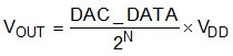
where:
- N is the resolution in bits, either 8 (DAC43701) or 10 (DAC53701).
- DAC_DATA is the decimal equivalent of the binary code that is loaded to the DAC register.
- DAC_DATA ranges from 0 to 2N – 1.
- VDD is used as the DAC reference voltage.