SLASED6D April 2016 – December 2017 DAC60004 , DAC70004 , DAC80004
PRODUCTION DATA.
- 1 Features
- 2 Applications
- 3 Description
- 4 Revision History
- 5 Device Comparison Table
- 6 Pin Configuration and Functions
- 7 Specifications
-
8 Detailed Description
- 8.1 Overview
- 8.2 Functional Block Diagram
- 8.3 Feature Description
- 8.4 Device Functional Modes
- 9 Application and Implementation
- 10Power Supply Recommendations
- 11Layout
- 12Device and Documentation Support
- 13Mechanical, Packaging, and Orderable Information
Package Options
Mechanical Data (Package|Pins)
Thermal pad, mechanical data (Package|Pins)
- DMD|14
Orderable Information
9 Application and Implementation
NOTE
Information in the following applications sections is not part of the TI component specification, and TI does not warrant its accuracy or completeness. TI’s customers are responsible for determining suitability of components for their purposes. Customers should validate and test their design implementation to confirm system functionality.
9.1 Application Information
9.2 Typical Application - Digitally Controlled Asymmetric Bipolar Output
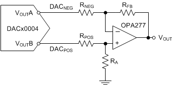
 Figure 58. Asymmetric Bipolar Output Block Diagram
9.2.1 Design Requirements
This design requires two channels of the DACx0004 to generate a bipolar output. The design is very flexible and allows for many different configurations. Typically, one channel is used to finely control the output, while the other is used to offset the output. The direction of the offset depends on which channel is used as an offset. DACPOS provides a positive offset and DACNEG has a negative offset.
9.2.2 Detailed Design Procedure
The output of each DAC can be modified via the digital interface and the gain of each output can be modified independently by changing the external resistors. In order for the gain of each offset to be independent, Equation 2 must be true.

The output voltage range, VOUT, is adjusted according to Equation 3. Keep in mind that Equation 3 is only true when Equation 2 is true.

Each DAC outputs a voltage from 0 to REFIN. As an example, if DACPOS gain is 1, DACNEG gain is 2 and RFB = 2 kΩ, then RPOS = 2 kΩ, RNEG = 1 kΩ and RA = 1 kΩ. With the correct digital implementation it gives the output an effective output range of ±15 V, with discrete 16-bit steps.
9.2.3 Application Curve
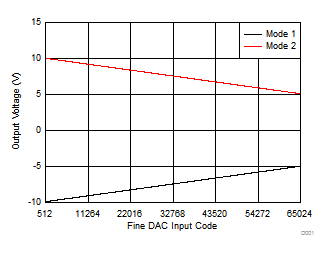
Figure 59 displays two different modes of operation. Mode 1 gains the output of DACNeg by a factor of 2 and maintains DACPOS at unity gain. Mode 2 reverses the gains of each stage to invert the system. These are just two examples of the types of outputs that can be achieved using this configuration.
 Figure 59. Output Voltage vs Fine DAC Input Code