SBAS439C August 2008 – July 2015 DAC8311 , DAC8411
PRODUCTION DATA.
- 1 Features
- 2 Applications
- 3 Description
- 4 Revision History
- 5 Device Comparison
- 6 Pin Configuration and Functions
- 7 Specifications
- 8 Detailed Description
- 9 Application and Implementation
- 10Power Supply Recommendations
- 11Layout
- 12Device and Documentation Support
- 13Mechanical, Packaging, and Orderable Information
Package Options
Mechanical Data (Package|Pins)
- DCK|6
Thermal pad, mechanical data (Package|Pins)
Orderable Information
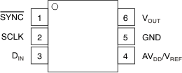
6 Pin Configuration and Functions
DCK Package
6-Pin SC70
Top View

Pin Functions
| PIN | I/O | DESCRIPTION | |
|---|---|---|---|
| NAME | NO. | ||
| AVDD/VREF | 4 | I | Power Supply Input, +2 V to +5.5 V. |
| DIN | 3 | I | Serial Data Input. Data is clocked into the 24-bit (DAC8411) or 16-bit (DAC8311) input shift register on the falling edge of the serial clock input. |
| GND | 5 | — | Ground reference point for all circuitry on the part. |
| SCLK | 2 | I | Serial Clock Input. Data can be transferred at rates up to 50 MHz. |
| SYNC | 1 | I | Level-triggered control input (active low). This is the frame sychronization signal for the input data. When SYNC goes low, it enables the input shift register and data are transferred in on the falling edges of the following clocks. The DAC is updated following the 24th (DAC8411) or 16th (DAC8311) clock cycle, unless SYNC is taken high before this edge, in which case the rising edge of SYNC acts as an interrupt and the write sequence is ignored by the DAC8x11. Refer to the DAC8311 and DAC8411SYNC Interrupt sections for more details. |
| VOUT | 6 | O | Analog output voltage from DAC. The output amplifier has rail-to-rail operation. |