SLAS476H March 2006 – June 2017 DAC8550
PRODUCTION DATA.
- 1 Features
- 2 Applications
- 3 Description
- 4 Revision History
- 5 Pin Configuration and Functions
- 6 Specifications
- 7 Detailed Description
- 8 Application and Implementation
- 9 Power Supply Recommendations
- 10Layout
- 11Device and Documentation Support
- 12Mechanical, Packaging, and Orderable Information
Package Options
Mechanical Data (Package|Pins)
- DGK|8
Thermal pad, mechanical data (Package|Pins)
Orderable Information
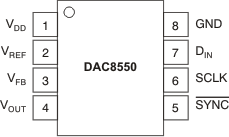
5 Pin Configuration and Functions
DGK Package
8-Pin VSSOP
Top View

Pin Functions
| PIN | TYPE | DESCRIPTION | |
|---|---|---|---|
| NAME | NO. | ||
| VDD | 1 | PWR | Power-supply input |
| VREF | 2 | I | Reference voltage input |
| VFB | 3 | I | Feedback connection for the output amplifier |
| VOUT | 4 | O | Analog output voltage from DAC. The output amplifier has rail-to-rail operation. |
| SYNC | 5 | I | Level-triggered control input (active LOW). This is the frame synchronization signal for the input data. When SYNC goes LOW, it enables the input shift register and data is transferred in on the falling edges of the following clocks. The DAC is updated following the 24th clock (unless SYNC is taken HIGH before this edge, in which case the rising edge of SYNC acts as an interrupt and the write sequence is ignored by the DAC8550). Schmitt-Trigger logic input. |
| SCLK | 6 | I | Serial clock input. Data can be transferred at rates up to 30 MHz Schmitt-Trigger logic input. |
| DIN | 7 | I | Serial data input. Data is clocked into the 24-bit input shift register on each falling edge of the serial clock input. Schmitt-Trigger logic input. |
| GND | 8 | GND | Ground reference point for all circuitry on the part |