SBVS012I December   2000  – September 2020 DCP010505B , DCP010505DB , DCP010507DB , DCP010512B , DCP010512DB , DCP010515B , DCP010515DB , DCP011512DB , DCP011515DB , DCP012405B , DCP012415DB

PRODUCTION DATA  

  1. Features
  2. Applications
  3. Description
  4. Revision History
  5. Pin Configuration and Functions
    1.     Pin Functions
  6. Specifications
    1. 6.1 Absolute Maximum Ratings
    2. 6.2 ESD Ratings
    3. 6.3 Recommended Operating Conditions
    4. 6.4 Thermal Information
    5. 6.5 Electrical Characteristics
    6. 6.6 Switching Characteristics
    7. 6.7 Typical Characteristics
  7. Detailed Description
    1. 7.1 Overview
    2. 7.2 Functional Block Diagrams
    3. 7.3 Feature Description
      1. 7.3.1  Isolation
        1. 7.3.1.1 Operation or Functional Isolation
        2. 7.3.1.2 Basic or Enhanced Isolation
        3. 7.3.1.3 Continuous Voltage
        4. 7.3.1.4 Isolation Voltage
        5. 7.3.1.5 Repeated High-Voltage Isolation Testing
      2. 7.3.2  Power Stage
      3. 7.3.3  Oscillator And Watchdog Circuit
      4. 7.3.4  Thermal Shutdown
      5. 7.3.5  Synchronization
      6. 7.3.6  Light Load Operation (< 10%)
      7. 7.3.7  Load Regulation (10% to 100%)
      8. 7.3.8  Construction
      9. 7.3.9  Thermal Management
      10. 7.3.10 Power-Up Characteristics
    4. 7.4 Device Functional Modes
      1. 7.4.1 Disable and Enable (SYNCIN Pin)
      2. 7.4.2 Decoupling
        1. 7.4.2.1 Ripple Reduction
        2. 7.4.2.2 Connecting the DCP01B in Series
        3. 7.4.2.3 Connecting the DCP01B in Parallel
  8. Application and Implementation
    1. 8.1 Application Information
    2. 8.2 Typical Application
      1. 8.2.1 Design Requirements
      2. 8.2.2 Detailed Design Procedure
        1. 8.2.2.1 Input Capacitor
        2. 8.2.2.2 Output Capacitor
        3. 8.2.2.3 SYNCIN Pin
      3. 8.2.3 DCP010505 Application Curves
      4. 8.2.4 PCB Design
      5. 8.2.5 Decoupling Ceramic Capacitors
      6. 8.2.6 Input Capacitor and the Effects of ESR
      7. 8.2.7 Ripple and Noise
        1. 8.2.7.1 Output Ripple Calculation Example
      8. 8.2.8 Dual DCP01B Output Voltage
      9. 8.2.9 Optimizing Performance
  9. Power Supply Recommendations
  10. 10Layout
    1. 10.1 Layout Guidelines
    2. 10.2 Layout Example
  11. 11Device and Documentation Support
    1. 11.1 Device Support
      1. 11.1.1 Device Nomenclature
    2. 11.2 Documentation Support
      1. 11.2.1 Related Documentation
    3. 11.3 Receiving Notification of Documentation Updates
    4. 11.4 Support Resources
    5. 11.5 Trademarks
    6. 11.6 Glossary
    7. 11.7 Electrostatic Discharge Caution
  12. 12Mechanical, Packaging, and Orderable Information

Package Options

Mechanical Data (Package|Pins)
Thermal pad, mechanical data (Package|Pins)
Orderable Information

Power-Up Characteristics

The DCP01B series of devices do not include a soft-start feature. Therefore, a high in-rush current during power up is expected. Refer to the DCPA1 series of devices for a 1-W, isolated, unregulated DC/DC converter module with soft start included. Figure 7-3 shows the typical start-up waveform for a DCP010505BP, operating from a 5-V input with no load on the output. Figure 7-4 shows the start-up waveform for a DCP010505BP starting up into a 10% load. Figure 7-5 shows the start-up waveform starting up into a full (100%) load.
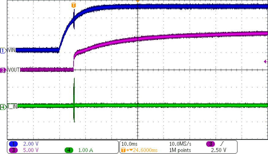
GUID-2BF27952-D6B3-4433-AE4B-E5780A9D382F-low.gifFigure 7-3 DCP010505BP Start-Up at No Load
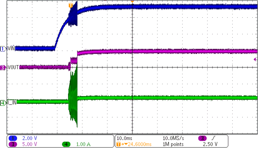
GUID-3C6E8372-A2E4-4BB8-A398-271AF6B40F02-low.gifFigure 7-5 DCP010505BP Start-Up at 100% Load
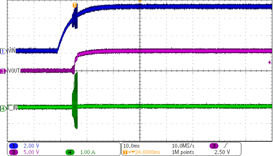
GUID-0861BE9A-11EC-405C-8326-44545538EBDA-low.gifFigure 7-4 DCP010505BP Start-Up at 10% Load