DLPS097A August 2017 – February 2023 DLP650NE
PRODUCTION DATA
- 1 Features
- 2 Applications
- 3 Description
- 4 Revision History
- 5 Pin Configuration and Functions
-
6 Specifications
- 6.1 Absolute Maximum Ratings
- 6.2 Storage Conditions
- 6.3 ESD Ratings
- 6.4 Recommended Operating Conditions
- 6.5 Thermal Information
- 6.6 Electrical Characteristics
- 6.7 Timing Requirements
- 6.8 Window Characteristics
- 6.9 System Mounting Interface Loads
- 6.10 Micromirror Array Physical Characteristics
- 6.11 Micromirror Array Optical Characteristics
- 6.12 Chipset Component Usage Specification
-
7 Detailed Description
- 7.1 Overview
- 7.2 Functional Block Diagram
- 7.3 Feature Description
- 7.4 Device Functional Modes
- 7.5 Optical Interface and System Image Quality Considerations
- 7.6 Micromirror Array Temperature Calculation
- 7.7 Micromirror Landed-On or Landed-Off Duty Cycle
- 8 Power Supply Requirements
- 9 Device Documentation Support
- 10Mechanical, Packaging, and Orderable Information
Package Options
Refer to the PDF data sheet for device specific package drawings
Mechanical Data (Package|Pins)
- FYE|350
Thermal pad, mechanical data (Package|Pins)
Orderable Information
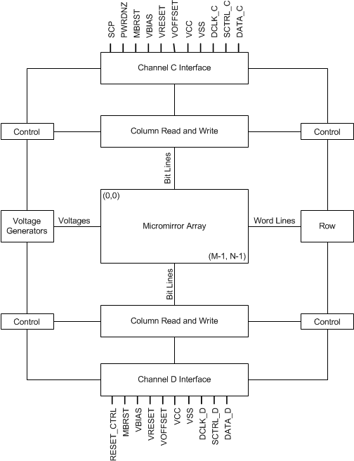
7.2 Functional Block Diagram
The main LVDS lines going to the DMD are connected via channel A and B. However, the LVDS lines come from channel C and D off the DLPC4430. Please refer to the DLPC4430 data sheet for more information.
For pin details
on Channels A, B, C, and D, refer to
GUID-E7B7574C-B5FF-45F3-A720-D3CAB64A881F.html#GUID-E7B7574C-B5FF-45F3-A720-D3CAB64A881F
and LVDS Interface section of Timing Requirements.