DLPS047B September 2014 – October 2015 DLPA2005
PRODUCTION DATA.
- 1 Features
- 2 Applications
- 3 Description
- 4 Revision History
- 5 Pin Configuration and Functions
- 6 Specifications
-
7 Detailed Description
- 7.1 Overview
- 7.2 Functional Block Diagram
- 7.3
Feature Description
- 7.3.1 DMD Regulators
- 7.3.2 RGB Strobe Decoder
- 7.3.3 LED Current Control
- 7.3.4 Maximum Led Currents and Efficiency Considerations
- 7.3.5 Calculating Inductor Peak Current
- 7.3.6 LED Current Accuracy
- 7.3.7 Transient Current Limiting
- 7.3.8 1.1-V Regulator (Buck Converter)
- 7.3.9 Measurement System
- 7.3.10
Protection Circuits
- 7.3.10.1 Thermal Warning (HOT) and Thermal Shutdown (TSD)
- 7.3.10.2 Low Battery Warning (BAT_LOW) and Undervoltage Lockout (UVLO)
- 7.3.10.3 DMD Regulator Fault (DMD_FLT)
- 7.3.10.4 V6V Power-Good (V6V_PGF) Fault
- 7.3.10.5 VLED Overvoltage (VLED_OVP) Fault
- 7.3.10.6 VLED Power Save Mode
- 7.3.10.7 V1V8 PG Failure
- 7.3.10.8 Interrupt Pin (INTZ)
- 7.3.10.9 SPI
- 7.3.11 Password Protected Registers
- 7.4 Device Functional Modes
- 7.5 Register Maps
- 8 Application and Implementation
- 9 Power Supply Recommendations
- 10Layout
- 11Device and Documentation Support
- 12Mechanical, Packaging, and Orderable Information
Package Options
Mechanical Data (Package|Pins)
- RSL|48
Thermal pad, mechanical data (Package|Pins)
- RSL|48
Orderable Information
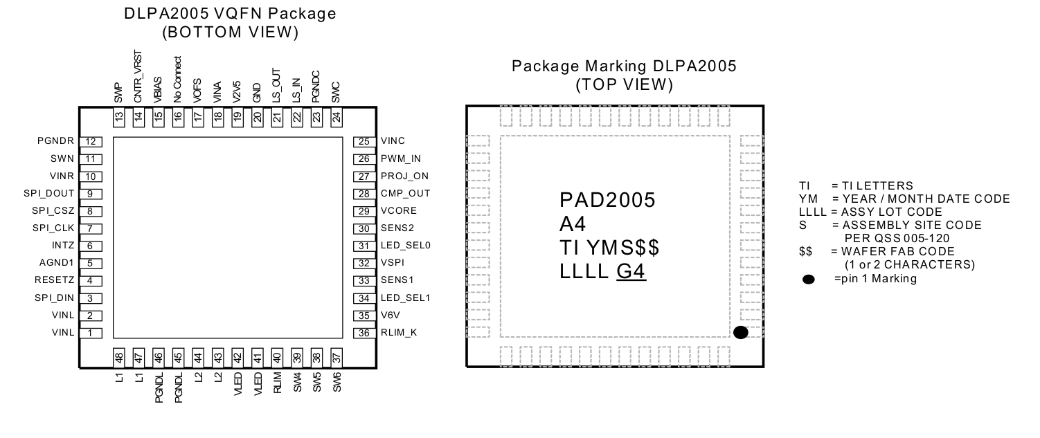
5 Pin Configuration and Functions

Pin Functions
| PIN | I/O | DESCRIPTION | |
|---|---|---|---|
| NAME | NUMBER | ||
| VINL | 1 | I | Power supply input for VLED BUCK-BOOST power stage. Connect to system power. |
| 2 | |||
| SPI_DIN | 3 | I | SPI data input |
| RESETZ | 4 | O | Reset output to the DLP system (active low). Pin is held low to reset DLP system. |
| AGND1 | 5 | GND | Analog ground. Connect to ground plane. |
| INTZ | 6 | O | Interrupt output signal (open drain). Connect to pullup resistor or short to ground. |
| SPI_CLK | 7 | I | Clock input for SPI interface |
| SPI_CSZ | 8 | I | SPI chip select (active low) |
| SPI_DOUT | 9 | O | SPI data output |
| VINR | 10 | I | Power supply input for DMD switch mode power supply (SMPS). Connect to system power. |
| SWN | 11 | I | Connection for the DMD SMPS-inductor (high-side switch). |
| PGNDR | 12 | GND | Power ground for DMD SMPS. Connect to ground plane. |
| SWP | 13 | O | Connection for the DMD SMPS-inductor (low-side switch). |
| CNTR_VRST | 14 | O | Connection to VRST for fast discharge function |
| VBIAS | 15 | O | VBIAS output rail. Connect to ceramic capacitor. |
| No Connect | 16 | I | Previously reference pin for the VRST regulator. On A4 design this reference is internal to DLPA2005 chip. |
| VOFS | 17 | O | VOFS output rail. Connect to ceramic capacitor. |
| VINA | 18 | POWER | Power supply input for sensitive analog circuitry |
| V2V5 | 19 | O | Internal supply filter pin for digital logic; typical 2.5 V |
| GND | 20 | GND | Ground connection to be connected to ground plane. |
| LS_OUT | 21 | O | Load switch |
| LS_IN | 22 | I | Load switch |
| PGNDC | 23 | GND | Power ground for VCORE BUCK |
| SWC | 24 | I/0 | Connection for 1.1-V BUCK inductor |
| VINC | 25 | I | Power supply input for VCORE BUCK power stage. Connect to system power. |
| PWM_IN | 26 | I | Reference voltage input for analog comparator. |
| PROJ_ON | 27 | I | Input signal to enable or disable the IC and DLP projector. |
| CMP_OUT | 28 | O | Analog-comparator output. |
| VCORE | 29 | I | VCORE BUCK converter feedback pin. |
| SENS2 | 30 | I | Input signal from temperature sensor. |
| LED_SEL0 | 31 | I | Digital input to the RGB Strobe Decoder |
| VSPI | 32 | I | Power supply input for SPI interface. Connect to system I/O voltage. |
| SENS1 | 33 | I | Input signal from light sensor. |
| LED_SEL1 | 34 | I | Digital input to the RGB Strobe Decoder |
| V6V | 35 | O | Internal supply filter pin for gate driver circuitry. Typical 6.25 V |
| RLIM_K | 36 | I | Kelvin sense connection to top side of LED current sense resistor. For best accuracy, route this trace directly to the top of the current sense resistor and separate it from the normal trace from the current sense resistor to the RLIM pins. |
| SW6 | 37 | O | Low-side MOSFET switch for LED cathode. Connect to RGB LED assembly. |
| SW5 | 38 | O | Low-side MOSFET switch for LED cathode. Connect to RGB LED assembly. |
| SW4 | 39 | O | Low-side MOSFET switch for LED cathode. Connect to RGB LED assembly. |
| RLIM | 40 | O | Connection to LED ‘current sense’ resistor. Bottom side of sense resistor is connected to GND. |
| VLED | 41 / 42 | O | VLED BUCK-BOOST converter output pin. |
| L2 | 43 / 44 | I | Connection for VLED BUCK-BOOST inductor. |
| PGNDL | 45 / 46 | GND | Power ground for VLED BUCK-BOOST. Connect to ground plane. |
| L1 | 47 / 48 | O | Connection for VLED BUCK-BOOST inductor. |