DLPS223A December 2021 – February 2023 DLPC4430
PRODUCTION DATA
- 1 Features
- 2 Applications
- 3 Description
- 4 Revision History
- 5 Pin Configuration and Functions
-
6 Specifications
- 6.1 Absolute Maximum Ratings
- 6.2 ESD Ratings
- 6.3 Recommended Operating Conditions
- 6.4 Thermal Information
- 6.5 Electrical Characteristics
- 6.6 System Oscillators Timing Requirements
- 6.7 Test and Reset Timing Requirements
- 6.8 JTAG Interface: I/O Boundary Scan Application Timing Requirements
- 6.9 Port 1 Input Pixel Timing Requirements
- 6.10 Port 3 Input Pixel Interface (via GPIO) Timing Requirements
- 6.11 DMD LVDS Interface Timing Requirements
- 6.12 Synchronous Serial Port (SSP) Interface Timing Requirements
- 6.13 Programmable Output Clocks Switching Characteristics
- 6.14 Synchronous Serial Port Interface (SSP) Switching Characteristics
- 6.15 JTAG Interface: I/O Boundary Scan Application Switching Characteristics
-
7 Detailed Description
- 7.1 Overview
- 7.2 Functional Block Diagram
- 7.3 Feature Description
- 7.4 Device Functional Modes
- 8 Application and Implementation
- 9 Power Supply Recommendations
- 10Layout
- 11Device and Documentation Support
- 12Mechanical, Packaging, and Orderable Information
Package Options
Mechanical Data (Package|Pins)
- ZPC|516
Thermal pad, mechanical data (Package|Pins)
Orderable Information
10.1.3 DMD Interface Considerations
High speed interface waveform quality and timing on the DLPC4430 controller (that is, the LVDS DMD Interface) is dependent on the total length of the interconnect system, the spacing between traces, the characteristic impedance, etch losses, and how well matched the lengths are across the interface. Thus ensuring positive timing margin requires attention to many factors.
As an example, DMD Interface system timing margin can be calculated as follows:
- Setup Margin = (DLPC4430 output setup) – (DMD input setup) – (PCB routing mismatch) – (PCB SI degradation)
- Hold-time Margin = (DLPC4430 output hold) – (DMD input hold) – (PCB routing mismatch) – (PCB SI degradation)
Where PCB SI degradation is signal integrity degradation due to PCB effects, which include simultaneously switching output (SSO) noise, cross-talk and inter-symbol interference (ISI) noise. The controller I/O timing parameters as well as DMD I/O timing parameters can be easily found in their corresponding data sheets. Similarly, PCB routing mismatch can be budgeted and met through controlled PCB routing. However, PCB SI degradation is not so straight forward.
In an attempt to minimize the signal integrity analysis, the following PCB design guidelines are provided as a reference of an interconnect system that satisfies both waveform quality and timing requirements (accounting for both PCB routing mismatch and PCB SI degradation). Variation from these recommendations may also work, but have to be confirmed with PCB signal integrity analysis or lab measurements
PDB Design:
| ● Configuration | Asymmetric Dual Stripline |
| ● Etch Thickness | 1.0 oz copper (1.2 mil) |
| ● Flex Etch Thickness | 0.5 oz copper (0.6 mil) |
| ● Single Ended Signal Impedance | 50 ohms (+/– 10%) |
| ● Differential Signal Impedance | 100 ohms differential (+/– 10%) |
PCB Stackup:
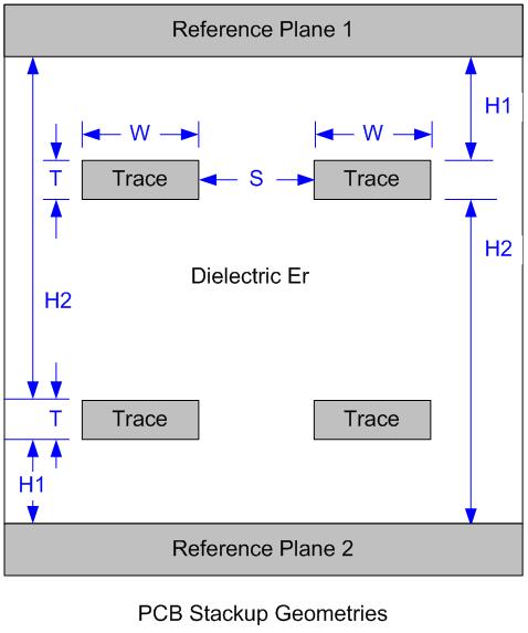
| ● Reference plane 1 is assumed to be a ground plane for proper return path | |
| ● Reference plane 2 is assumed to be the I/O power plane or ground | |
| ● Dielectric FR4, (Er): | 4.2 (nominal) |
| ● Signal trace distance to reference plane 1 (H1) | 5.0 mil (nominal) |
| ● Signal trace distance to reference plane 2 (H2) | 34.2 mil (nominal) |
 Figure 10-2 PCB Stackup Geometries
| PARAMETER | APPLICATION | SINGLE-ENDED SIGNAL | DIFFERENTIAL PAIRS | UNIT |
|---|---|---|---|---|
| Line width (W)(1) | Escape Routing in Ball Field | 4 (0.1) | 4 (0.1) | mil (mm) |
| PCB Etch Data or Control | 7 (0.18) | 4.25 (0.11) | mil (mm) | |
| PCB Etch Clocks | 7 (0.18) | 4.25 (0.11) | mil (mm) | |
| Minimum Line spacing to other signals (S) | Escape Routing in Ball Field | 4 (0.1) | 4 (0.1) | mil (mm) |
| PCB Etch Data or Control | 10 (0.25) | 20 (0.51) | mil (mm) | |
| PCB Etch Clocks | 20 (0.51) | 20 (0.51) | mil (mm) |
| SIGNAL GROUP LENGTH MATCHING | ||||
|---|---|---|---|---|
| I/F | SIGNAL GROUP | REFERENCE SIGNAL | MAX MISMATCH | UNIT |
| DMD (LVDS) | SCA_P,SCA_N, DDA_P(15:0), DDA_N(15:0) | DCKA_P, DCKA_N | +/-150 (+/–3.81) | mil (mm) |
| DMD (LVDS) | SCB_P,SCB_N, DDB_P(15:0), DDB_N(15:0) | DCKB_P, DCKB_N | +/-150 (+/–3.81) | mil (mm) |
Number of layer changes:
- Single ended signals: Minimize
- Differential signals: Individual differential pairs can be routed on different layers but the signals of a given pair typically does not change layers.
Termination requirements:
- DMD
Interface—None,
the DMD receiver is differentially terminated to 100 ohms internally
Connector (DMD-LVDS I/F bus only)—High Speed Connectors that meet the following requirements must be used:
● Differential Crosstalk <5 % ● Differential Impedance 75 ohms–125 ohms
Routing requirements for right angle connectors:
When using right angle connectors, P-N pairs have to be routed in same row to minimize delay mismatch and propagation delay difference for each row has to be accounted for on associated PCB etch lengths.