SLVSDN2E January   2018  – March 2021 DRV10974

PRODUCTION DATA  

  1. Features
  2. Applications
  3. Description
  4. Revision History
  5. Pin Configuration and Functions
  6. Specifications
    1. 6.1 Absolute Maximum Ratings
    2. 6.2 ESD Ratings
    3. 6.3 Recommended Operating Conditions
    4. 6.4 Thermal Information
    5. 6.5 Electrical Characteristics
    6. 6.6 Typical Characteristics
  7. Detailed Description
    1. 7.1 Overview
    2. 7.2 Functional Block Diagram
    3. 7.3 Feature Description
      1. 7.3.1 Speed Input and Control
      2. 7.3.2 Motor Direction Change
      3. 7.3.3 Motor-Frequency Feedback (FG)
      4. 7.3.4 Lock Detection
        1. 7.3.4.1 Lock Kt Measure
        2. 7.3.4.2 Lock No Motor
        3. 7.3.4.3 Lock Open Loop Abnormal
        4. 7.3.4.4 Lock BEMF Abnormal
        5. 7.3.4.5 Lock Closed Loop Abnormal
        6. 7.3.4.6 Lock Speed Abnormal
      5. 7.3.5 Soft Current-Limit
      6. 7.3.6 Short-Circuit Current Protection
      7. 7.3.7 Overtemperature Protection
      8. 7.3.8 Undervoltage Protection
    4. 7.4 Device Functional Modes
      1. 7.4.1 Spin-Up Settings
        1. 7.4.1.1 Motor Start
        2. 7.4.1.2 Initial Speed Detect
        3. 7.4.1.3 Align
      2. 7.4.2 Open-Loop Acceleration
      3. 7.4.3 Start-Up Current Sensing
      4. 7.4.4 Closed Loop
      5. 7.4.5 Control Advance Angle
  8. Application and Implementation
    1. 8.1 Application Information
    2. 8.2 Typical Application
      1. 8.2.1 Design Requirements
      2. 8.2.2 Detailed Design Procedure
      3. 8.2.3 Application Curves
  9. Power Supply Recommendations
  10. 10Layout
    1. 10.1 Layout Guidelines
    2. 10.2 Layout Example
  11. 11Device and Documentation Support
    1. 11.1 Device Support
    2. 11.2 Receiving Notification of Documentation Updates
    3. 11.3 Support Resources
    4. 11.4 Trademarks
    5. 11.5 Electrostatic Discharge Caution
    6. 11.6 Glossary
  12. 12Mechanical, Packaging, and Orderable Information

Package Options

Mechanical Data (Package|Pins)
Thermal pad, mechanical data (Package|Pins)
Orderable Information

Typical Application

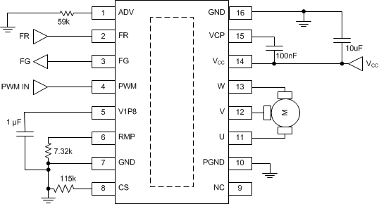
GUID-F077F803-4940-412F-9092-A26D73C1B28C-low.gifFigure 8-1 Typical Application Schematic
Table 8-1 Recommended External Components
NODE 1NODE 2COMPONENT
VCCGND10-μF, 25-V ceramic capacitor tied from VCC to ground
VCPVCC100-nF, 10-V ceramic capacitor tied from VCP to VCC
V1P8GND1-μF ±30%, 6.3-V ceramic capacitor tied from V1P8 to ground
RMPGND1%, 1/8 watt resistor tied from RMP to ground to set the desired acceleration profile
CSGND1%, 1/8-watt resistor tied from CS to ground to set the desired current limit
ADVGND1%, 1/8-watt resistor tied from ADV to ground to set the desired lead angle (time)