SBOS094B January 1998 – December 2014 DRV134 , DRV135
PRODUCTION DATA.
- 1 Features
- 2 Applications
- 3 Description
- 4 Simplified Schematic
- 5 Revision History
- 6 Pin Configuration and Functions
- 7 Specifications
- 8 Detailed Description
- 9 Application and Implementation
- 10Power Supply Recommendations
- 11Layout
- 12Device and Documentation Support
- 13Mechanical, Packaging, and Orderable Information
Package Options
Mechanical Data (Package|Pins)
- D|8
Thermal pad, mechanical data (Package|Pins)
Orderable Information
9 Application and Implementation
NOTE
Information in the following applications sections is not part of the TI component specification, and TI does not warrant its accuracy or completeness. TI’s customers are responsible for determining suitability of components for their purposes. Customers should validate and test their design implementation to confirm system functionality.
9.1 Application Information
Decoupling capacitors placed close to the device pins are strongly recommended in applications with noisy or high impedance power supplies.
For best system performance, it is recommended that a high input-impedance difference amplifier be used as the receiver. Used with the INA134 (G = 0 dB) or the INA137 (G = ±6 dB) differential line receivers, the DRV134 forms a complete solution for driving and receiving audio signals, replacing input and output coupling transformers commonly used in professional audio systems (Figure 29). When used with the INA137 (G = –6 dB) overall system gain is unity.
9.2 Typical Application
9.2.1 Cable Driving Application
The DRV134 is capable of driving large signals into 600-Ω loads over long cables. Low impedance shielded audio cables such as the standard Belden 8451 or 9452 (or similar) are recommended, especially in applications where long cable lengths are required.
For applications with large dc cable offset errors, a 10-µF electrolytic nonpolarized blocking capacitor at each sense pin is recommended as shown in Figure 29.
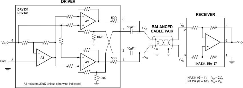 Figure 29. Complete Audio Driver and Receiver Circuit
9.2.1.1 Design Requirements
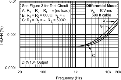
Consider a design with the goal of differentially transmitting a single ended signal of up to 22.2 dBu through 500 ft of cable with no load at the receiving side. The signal at the end of the cable should have no more than 0.002 percent of total harmonic distortion plus noise (THD+N) at 10 kHz and less than 0.0005 percent of THD+N for frequencies between 20 Hz and 1 kHz.
The system is required to put out a single ended signal 0 dB with respect to the input signal and accommodate inputs with peak to RMS ratios of up to 1.5 for the maximum 22.2 dBu range established above.
9.2.1.2 Detailed Design Procedure
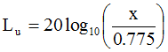
The dBu is a common unit of measurement for input sensitivity and output level of professional audio equipment. A 0 dBu signal dissipates 1 mW into a 600-Ω resistive load; therefore, a 0 dBu signal corresponds to approximately 0.775 VRMS. Equation 1 shows the relationship between the signal level in dBu (denoted by Lu) and the signal level in VRMS (denoted by x).
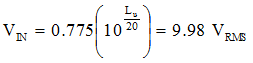
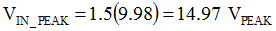
For this design, the single ended input signal of 22.2 dBu corresponds to 9.98 VRMS as shown in Equation 2.
Given that the system must accommodate for 22.2 dBu signals with up to 1.5 of peak to RMS ratio, the maximum peak input signal is 14.97 VPEAK as calculated in Equation 3.
The DRV134 is chosen to convert the single ended input signal into a differential signal and the outputs of the DRV134 will be connected to one end of the 500 ft cable. In order to prevent clipping and distortion of the input signal, the power supply rails for the DRV134 are chosen as 3 V above and below the peak calculated in Equation 3. The 3 V margin is derived from the output voltage swing specification given in the Electrical Characteristics table. The supplies selected are 18 V for V+ and –18 V for V–.
Finally, the INA137 is used at the end of the 500 ft cable in order to convert the differential signal output of the DRV134 into a single ended signal that is 0 dB with respect to the input signal.
Figure 30 shows the system diagram.
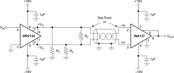 Figure 30. Diagram of System Based on DRV134 and INA137