SBOS094B January 1998 – December 2014 DRV134 , DRV135
PRODUCTION DATA.
- 1 Features
- 2 Applications
- 3 Description
- 4 Simplified Schematic
- 5 Revision History
- 6 Pin Configuration and Functions
- 7 Specifications
- 8 Detailed Description
- 9 Application and Implementation
- 10Power Supply Recommendations
- 11Layout
- 12Device and Documentation Support
- 13Mechanical, Packaging, and Orderable Information
Package Options
Mechanical Data (Package|Pins)
- D|8
Thermal pad, mechanical data (Package|Pins)
Orderable Information
8 Detailed Description
8.1 Overview
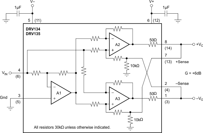
The DRV134 and DRV135 consist of an input inverter driving a cross- coupled differential output stage with 50 Ω series output resistors. Characterized by low differential-mode output impedance (50 Ω) and high common-mode output impedance (1.6 kΩ), the DRV134 and DRV135 are ideal for audio applications.
Excellent internal design and layout techniques provide low signal distortion, high output level (27 dBu), and a low noise floor (–98 dBu). Laser trimming of thin film resistors assures excellent output common-mode rejection (OCMR) and signal balance ratio (SBR). In addition, low dc voltage offset reduces errors and minimizes load currents.
The Functional Block Diagram section shows a detailed block diagram of the DRV134 and DRV135.
8.2 Functional Block Diagram
8.3 Feature Description
8.3.1 Audio Performance
The DRV134 and DRV135 were designed for enhanced ac performance. Very low distortion, low noise, and wide bandwidth provide superior performance in high quality audio applications. Laser-trimmed matched resistors provide optimum output common-mode rejection (typically 68dB), especially when compared to circuits implemented with op amps and discrete precision resistors. In addition, high slew rate (15 V/μs) and fast settling time (2.5 μs to 0.01%) ensure excellent dynamic response.
The DRV134 and DRV135 have excellent distortion characteristics. As shown in the distortion data provided in the Typical Characteristics section, THD+Noise is below 0.003% throughout the audio frequency range under various output conditions. Both differential and single-ended modes of operation are shown. In addition, the optional 10μF blocking capacitors used to minimize VOCM errors have virtually no effect on performance. Measurements were taken with an Audio Precision System One (with the internal 80 kHz noise filter) using the THD test circuit shown in Figure 24.
Up to approximately 10 kHz, distortion is below the measurement limit of commonly used test equipment. Furthermore, distortion remains relatively constant over the wide output voltage swing range (approximately 2.5 V from the positive supply and 1.5 V from the negative supply). A special output stage topology yields a design with minimum distortion variation from lot-to-lot and unit-to-unit. Furthermore, the small and large signal transient response curves demonstrate the stability under load of the DRV134 and DRV135.
 Figure 24. Distortion Test Circuit
8.3.2 Output Common-Mode Rejection
Output common-mode rejection (OCMR) is defined as the change in differential output voltage due to a change in output common-mode voltage. When measuring OCMR, VIN is grounded and a common-mode voltage, VCM, is applied to the output as shown in Figure 25. Ideally no differential mode signal (VOD) should appear. However, a small mode-conversion effect causes an error signal whose magnitude is quantified by OCMR.
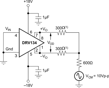 Figure 25. Output Common-Mode Rejection Test Circuit
8.3.3 Signal Balance Ratio
Signal balance ratio (SBR) measures the symmetry of the output signals under loaded conditions. To measure SBR an input signal is applied and the outputs are summed as shown in Figure 26. VOUT should be zero since each output ideally is exactly equal and opposite. However, an error signal results from any imbalance in the outputs. This error is quantified by SBR. The impedances of the DRV134 and DRV135’s output stages are closely matched by laser trimming to minimize SBR errors. In an application, SBR also depends on the balance of the load network.
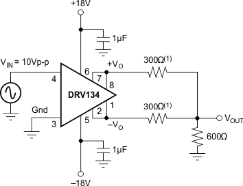 Figure 26. Signal Balance Ratio Test Circuit
8.4 Device Functional Modes
8.4.1 Differential-Output Mode
In differential-output mode, the DRV134 (and DRV135 in SO-8 package) converts a single-ended, ground-referenced input to a floating differential output with +6 dB gain (G = 2). Figure 27 shows the basic connections required for operation in differential-output mode.
Normally, +VO is connected to +Sense, –VO is connected to –Sense, and the outputs are taken from these junctions as shown in Figure 27.
Figure 27. Basic Connections for Differential-Output Mode
8.4.2 Single-Ended Mode
The DRV134 can be operated in single-ended mode without degrading output drive capability. Single-ended operation requires that the unused side of the output pair be grounded (both the VO and Sense pins) to a low impedance return path. Gain remains +6 dB. Grounding the negative outputs as shown in Figure 28 results in a non-inverted output signal (G = +2) while grounding the positive outputs gives an inverted output signal (G = –2).
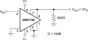 Figure 28. Typical Single-Ended Application
For best rejection of line noise and hum differential mode operation is recommended. However, single-ended performance is adequate for many applications. In general single ended performance is comparable to differential mode (see THD+N typical performance curves), but the common mode and noise rejection inherent in balanced-pair systems is lost.