SLVSCV1E September   2015  – February 2017 DRV3205-Q1

PRODUCTION DATA.  

  1. Features
  2. Applications
  3. Description
  4. Revision History
  5. Pin Configuration and Functions
  6. Specifications
    1. 6.1 Absolute Maximum Ratings
    2. 6.2 ESD Ratings
    3. 6.3 Recommended Operating Conditions
    4. 6.4 Thermal Information
    5. 6.5 Electrical Characteristics
    6. 6.6 Serial Peripheral Interface Timing Requirements
    7. 6.7 Typical Characteristics
  7. Detailed Description
    1. 7.1 Overview
    2. 7.2 Functional Block Diagram
    3. 7.3 Programming
      1. 7.3.1 SPI
        1. 7.3.1.1 Address Mode Transfer
          1. 7.3.1.1.1 SPI Address Transfer Phase
        2. 7.3.1.2 SPI Data Transfer Phase
        3. 7.3.1.3 Device Data Response
    4. 7.4 Register Maps
  8. Application and Implementation
    1. 8.1 Application Information
    2. 8.2 Typical Application
      1. 8.2.1 Three-Phase Motor Drive-Device for Automotive Application
    3. 8.3 System Example
  9. Power Supply Recommendations
  10. 10Layout
    1. 10.1 Layout Guidelines
    2. 10.2 Layout Example
  11. 11Device and Documentation Support
    1. 11.1 Documentation Support
      1. 11.1.1 Related Documentation
    2. 11.2 Receiving Notification of Documentation Updates
    3. 11.3 Community Resources
    4. 11.4 Trademarks
    5. 11.5 Electrostatic Discharge Caution
    6. 11.6 Glossary
  12. 12Mechanical, Packaging, and Orderable Information

Package Options

Mechanical Data (Package|Pins)
Thermal pad, mechanical data (Package|Pins)
Orderable Information

Application and Implementation

NOTE

Information in the following applications sections is not part of the TI component specification, and TI does not warrant its accuracy or completeness. TI’s customers are responsible for determining suitability of components for their purposes. Customers should validate and test their design implementation to confirm system functionality.

Application Information

The DRV3205-Q1 is a predriver for automotive applications featuring three-phase brushless DC-motor control. Because this device has a boost regulator for charging high-side gates, it can handle gate charges of 250 nC. A boost converter allows full control on the power-stages even for a low battery voltage down to 4.75 V.

Typical Application

Three-Phase Motor Drive-Device for Automotive Application

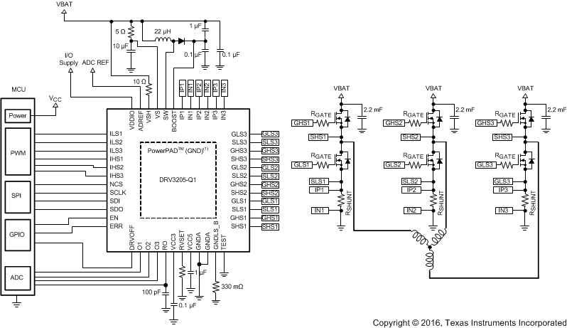
DRV3205-Q1 typ_app_LVSCV1.gif
This schematic of the DRV3205-Q1 48-pin HTQFP does not provide a true representation of physical pin locations.
Use same supply from the TPS6538x as the supply used for the MCU IO.
Resistor not required for reverse protected battery.
L1 = B82442A1223K000 INDUCTOR, SMT, 22 uH, 10%, 480 mA). The maximum inductor current must be more than VGNDLS_B / 330 mΩ.
D1 = SS28 (DIODE, SMT, SCHOTTKY, 80 V, 2 A). A fast recovery diode is recommended.
QxHS, QxLS = IRFS3004PBF (HEXFET, N-CHANNEL, POWER MOSFET, D2PACK)
Rshunt1 and Rshunt2 = BVR-Z-R0005 (RES, SMT, 4026, PRECISION POWER, 0.0005 Ω, 1%, 5 W)
Rgate = Must be adjust based on system requirement such as EMI, Slew rate, and power
Figure 17. Typical Application Diagram

System Example

Figure 18 shows a typical system example for an electric power-steering system.
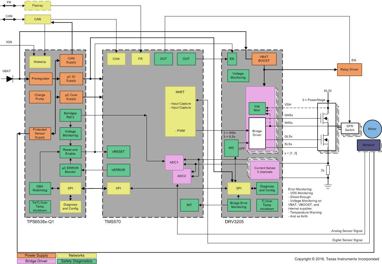
DRV3205-Q1 elect_pwr_steering_LVSCV1.gif Figure 18. Typical System – Electrical Power Steering Example