SBOS814 December 2016 DRV401-Q1
PRODUCTION DATA.
- 1 Features
- 2 Applications
- 3 Description
- 4 Revision History
- 5 Pin Configuration and Functions
- 6 Specifications
-
7 Detailed Description
- 7.1 Overview
- 7.2 Functional Block Diagram
- 7.3
Feature Description
- 7.3.1 Magnetic Probe (Sensor) Interface
- 7.3.2 PWM Processing
- 7.3.3 Compensation Driver
- 7.3.4 External Compensation Coil Driver
- 7.3.5 Shunt Sense Amplifier
- 7.3.6 Over-Range Comparator
- 7.3.7 Voltage Reference
- 7.3.8 Demagnetization
- 7.3.9 Power-On and Brownout
- 7.3.10 Error Conditions
- 7.3.11 Protection Recommendations
- 7.4 Device Functional Modes
- 8 Application and Implementation
- 9 Power Supply Recommendations
- 10Layout
- 11Device and Documentation Support
- 12Mechanical, Packaging, and Orderable Information
Package Options
Mechanical Data (Package|Pins)
- RGW|20
Thermal pad, mechanical data (Package|Pins)
- RGW|20
Orderable Information
10 Layout
10.1 Layout Guidelines
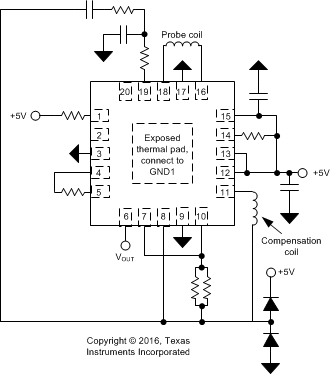
The typical device configuration is shown in Figure 42. The DRV401-Q1 operates with relatively large currents and fast current pulses, and offers wide-bandwidth performance. The device is often exposed to large distortion energy from the primary signal and the operating environment. Therefore, the wiring layout must provide shielding and low-impedance connections between critical points.
Use low-ESR capacitors for power-supply decoupling. Use a combination of a small capacitor and a large capacitor with a 1-μF or larger value. Use low-impedance tracks to connect the capacitors to the pins.
Both grounds must be connected to a local ground plane. Both supplies can be connected together; however, best results are achieved with separate decoupling (to the local GND plane) and ferrite beads in series with the main supply. The ferrite beads decouple the DRV401-Q1 device, reducing interaction with other circuits powered from the same supply voltage source.
The reference output is referred to GND2. A low-impedance, star-type connection is required to avoid the driver current and the probe current modulating the voltage drop on the ground track.
The connection wires of the difference amplifier to the shunt must be low resistance and of equal length. For best accuracy, avoid current in this connection. Consider using a Kelvin Contact-type connection. The required resistance value may be set using two resistors.
Wires and PCB traces for S1 and S2 must be close or twisted. ICOMP1 and ICOMP2 must be wired close together. To avoid capacitive coupling, run a ground shield between the S1/S2 and ICOMP wire pair or keep them distant from each other.
The compensation driver outputs (ICOMP) are low frequency only. However, the primary signal (with high-frequency content present) is coupled into the compensation winding, the shunt, and the difference amplifier. TI recommends a careful layout.
The REFOUT and VOUT output drives some capacitive loads, but avoid large direct capacitive loads; these loads increase internal pulse currents. Given the wide bandwidth of the differential amplifier, isolate any large capacitive load with a small series resistor. A small capacitor (in the pF range) improves the transient response on a high resistive load.
The exposed thermal pad on the bottom of the package must be soldered to GND because the thermal pad is internally connected to the substrate, which must be connected to the most negative potential. Solder the exposed pad to the PCB to provide structural integrity and long-term reliability.
10.2 Layout Example
 Figure 50. DRV401-Q1 Layout Example (RGW Package)
10.3 Power Dissipation
Using the thermally-enhanced VQFN package dramatically reduces the thermal impedance from junction to case. This package is constructed using a down-set lead frame that the die is mounted on. This arrangement results in the lead frame exposed as a thermal pad on the underside of the package. Because this thermal pad has direct thermal contact with the die, excellent thermal performance can be achieved by providing a good thermal path away from the thermal pad.
The two outputs (ICOMP1 and ICOMP2) are linear outputs. Therefore, the power dissipation on each output is proportional to the current multiplied by the internal voltage drop on the active transistor. For ICOMP1 and ICOMP2, this internal voltage drop is the voltage drop to VDD2 or GND, according to the current-conducting side of the output.
Output short-circuits are particularly critical for the driver because the full supply voltage can be seen across the conducting transistor, and the current is not limited by anything other than the current density limitation of the FET. Permanent damage to the device may occur.
The DRV401-Q1 does not include temperature protection or thermal shutdown.