SBOS814 December 2016 DRV401-Q1
PRODUCTION DATA.
- 1 Features
- 2 Applications
- 3 Description
- 4 Revision History
- 5 Pin Configuration and Functions
- 6 Specifications
-
7 Detailed Description
- 7.1 Overview
- 7.2 Functional Block Diagram
- 7.3
Feature Description
- 7.3.1 Magnetic Probe (Sensor) Interface
- 7.3.2 PWM Processing
- 7.3.3 Compensation Driver
- 7.3.4 External Compensation Coil Driver
- 7.3.5 Shunt Sense Amplifier
- 7.3.6 Over-Range Comparator
- 7.3.7 Voltage Reference
- 7.3.8 Demagnetization
- 7.3.9 Power-On and Brownout
- 7.3.10 Error Conditions
- 7.3.11 Protection Recommendations
- 7.4 Device Functional Modes
- 8 Application and Implementation
- 9 Power Supply Recommendations
- 10Layout
- 11Device and Documentation Support
- 12Mechanical, Packaging, and Orderable Information
Package Options
Mechanical Data (Package|Pins)
- RGW|20
Thermal pad, mechanical data (Package|Pins)
- RGW|20
Orderable Information
7 Detailed Description
7.1 Overview
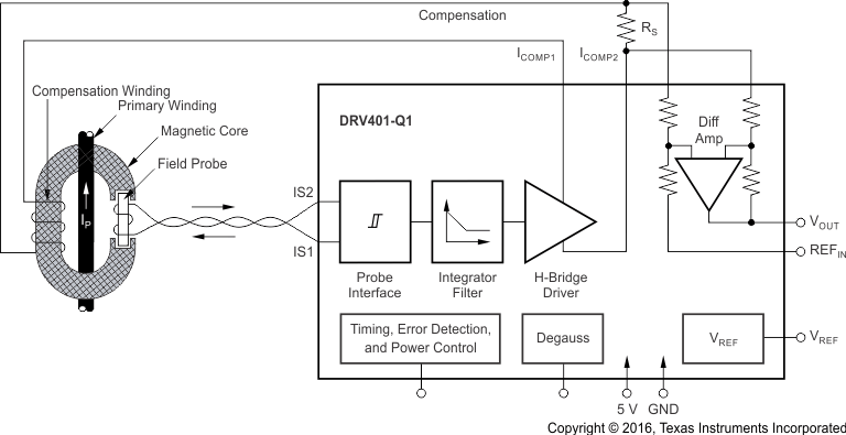
Closed-loop current sensors measure current over wide frequency ranges, including dc. These types of devices offer a contact-free method, as well as excellent galvanic isolation performance combined with high resolution, accuracy, and reliability. The DRV401-Q1 is a complete sensor signal conditioning circuit that directly connects to the current sensor, providing all necessary functions for the sensor operation.
7.2 Functional Block Diagram
7.3 Feature Description
The DRV401-Q1 operates from a single 5-V supply. The DRV401-Q1 is a complete sensor signal conditioning circuit that directly connects to the current sensor, providing all necessary functions for the sensor operation. The DRV401-Q1 device provides magnetic field probe excitation, signal conditioning, and compensation coil driver amplification. In addition, the device detects error conditions and handles overload situations. A precise differential amplifier allows translation of the compensation current into an output voltage using a small shunt resistor. A buffered voltage reference is used for comparator, analog-to-digital converter (ADC), or bipolar zero reference voltages.
Dynamic error correction ensures high dc precision over temperature and long-term accuracy. The DRV401-Q1 uses analog signal conditioning, and the internal loop filter and integrator are switched capacitor-based circuits. Therefore, the DRV401-Q1 device allows combination with high-precision sensors for exceptional accuracy and resolution.
A demagnetization cycle initiates on demand or on power-up. The cycle reduces offset and restores high performance after a strong overload condition. An internal clock and counter logic generate the degauss function. The same clock controls power-up, overload detection and recovery, error, and time-out conditions.
The DRV401-Q1 device is built on a highly reliable CMOS process. Unique protection cells at critical connections enable the design to handle inductive energy.
7.3.1 Magnetic Probe (Sensor) Interface
The magnetic field probe consists of an inductor wound on a soft magnetic core. The probe is connected between pins IS1 and IS2 of the probe driver that applies approximately 5 V (the supply voltage) through resistors across the probe coil, as shown in Figure 36.
Typically, the probe core reaches saturation at a current of 28 mA, as shown in Figure 36. The comparator is connected to VREF by approximately 0.5 V. A current comparator detects the saturation and inverts the excitation voltage polarity, causing the probe circuit to oscillate in a frequency range of 250 kHz to 550 kHz. The oscillating frequency is a function of the magnetic properties of the probe core and the coil.
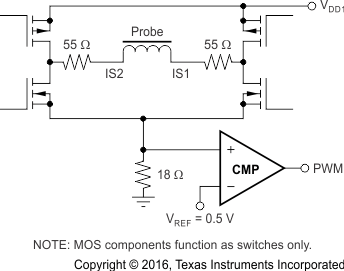
The current rise rate is a function of the coil inductance: dI = L × V × dT. However, the inductance of the field probe is low while the core material is in saturation (the horizontal part of the hysteresis curve) and is high at the vertical part of the hysteresis curve. The resulting inductance and the series resistance determine the output voltage and current versus time performance characteristic.
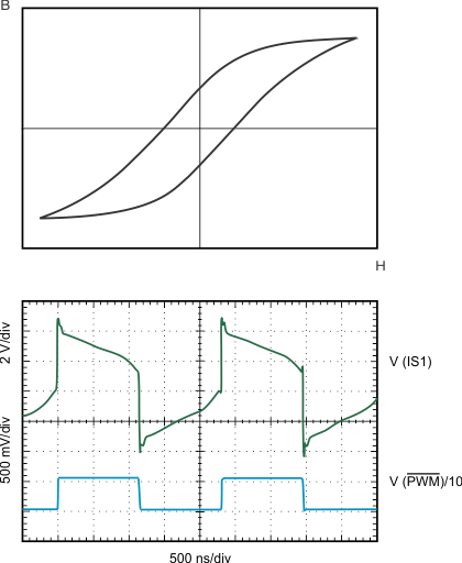
Without external magnetic influence, the duty cycle is exactly 50% because of the inherent symmetry of the magnetic hysteresis; the probe inductor is driven from −B saturation through the high inductance range to +B saturation and back again in a time-symmetric manner, as shown in Figure 37.
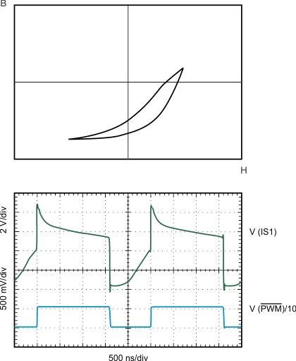
If the core material is magnetized in one direction, a long and a short charge time result because the probe current through the inductors generates a field that subtracts or adds to the flux in the probe core, driving the probe core out of saturation or further into saturation, as shown in Figure 38. The current into the probe is limited by the voltage drops across the probe driver resistors.
The DRV401-Q1 device continuously monitors the logic magnetic flux polarity state. In the case of distortion noise and excessive overload that can fully saturate the probe, the overload control circuit recovers the probe loop. During an overload condition, the probe oscillation frequency increases to approximately 1.6 MHz until limited by the internal timing control.
In an overload condition, the compensation current (ICOMP) driver cannot deliver enough current into the sensor secondary winding, so the magnetic flux in the sensor main core becomes uncompensated.
The transition from normal operation to overload happens slowly because the inherent sensor transformer characteristics induce the initial primary current step, as shown in Figure 39. As the transformer-induced secondary current starts to decay, the compensation feedback driver increases the output voltage to maintain the sensor core flux compensation at zero.
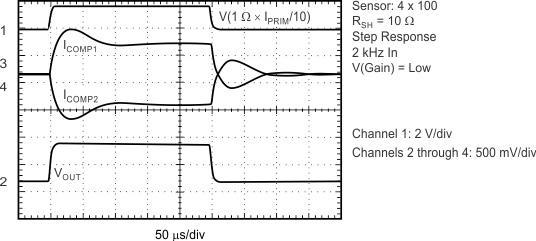
When the system compensation loop reaches the driving limit, the rising magnetic flux causes one of the probe pulse-width modulator (PWM) half-periods to become shorter. The minimum half-period of the probe oscillation is limited by the internal timing to 280 ns, based on the properties of the VAC magnetic sensors. After three consecutive cycles of the same half-period being shorter than 280 ns, the DRV401-Q1 device enters overload-latch mode. The device stores the ICOMP driver output signal polarity and continues producing the skewed-duty cycle PWM signal. This action prevents the loss of compensation signal polarity information during strong overloads. In this case, both PWM half-periods are short and approximately equal, because the field probe stays completely in one of the saturated regions.
The overload-latch condition is removed after the primary current goes low enough for the ICOMP driver to compensate, and both half-periods of the probe driver oscillation become longer than 280 ns (the field probe comes out of the saturated region).
Peak voltages and currents generate during normal operations and overload conditions. Both probe connection pins are internally protected against coupled energy from the magnetic core. Wiring between probe and device inputs must be short and guarded against interference, as shown in the Layout Guidelines section.
For reliable operation, error detection circuits monitor the probe operation:
- If the probe driver comparator (CMP) output stays low longer than 32 μs, the ERROR flag asserts active, and the compensation current (ICOMP) is set to zero.
- If the probe driver period is less than 275 ns on three consecutive pulses, the ERROR flag asserts active.
See the Error Conditions section for more details.
7.3.2 PWM Processing
The PWM and PWM outputs represent the probe output signal as a differential PWM signal. The signal drives external circuitry and is used for synchronous ripple reduction. The PWM signal from the probe excitation and sense stage is internally connected to a high-performance, switched-capacitor integrator followed by an integrating-differentiating filter. The filter converts the PWM signal into a filtered delta signal and prepares the PWM signal to drive the analog compensation coil driver. The gain roll-off frequency of the filter stage provides high dc gain and loop stability. If additional gain is added from external circuitry, the internal gain is reduced by 8 dB, which asserts the GAIN pin high, as shown in the External Compensation Coil Driver section.
7.3.3 Compensation Driver
The compensation coil driver provides the driving current for the compensation coil. A fully-differential driver stage offers high signal voltages to overcome the wire resistance of the coil with a 5-V supply. The compensation coil is connected between ICOMP1 and ICOMP2, generating an analog voltage across the coil (shown in Figure 39) that turns into current from the wire resistance (and eventually from the inductance). The compensation current represents the primary current transformed by the turns ratio. A shunt resistor is connected in this loop and the high-precision difference amplifier translates the voltage from the shunt to an output voltage.
Both compensation driver outputs provide low impedance over a wide frequency range to ensure smooth transitions between the closed-loop compensation frequency range and the high-frequency range, where the primary winding directly couples the primary current into the compensation coil at a rate set by the winding ratio.
The two compensation driver outputs are designed with protection circuitry to handle inductive energy. However, additional external protection diodes may be necessary for high-current sensors.
For reliable operation, a wire break in the compensation circuit can be detected. If the feedback loop is broken, the integrating filter drives the ICOMP1 and ICOMP2 outputs to the opposite rails. With one of these pins coming within 300 mV to ground, a comparator tests for a minimum current flowing between ICOMP1 and ICOMP2. If the current stays below the threshold current level for a minimum of 100 μs, the ERROR pin is asserted active (low). The threshold current level for the test is less than 57 mA at 25°C and 65 mA at −40°C if the ICOMP pins are fully railed, as shown in the Typical Characteristics section.
For sensors with high winding resistance (compensation coil resistance + RSHUNT) or that are connected to an external compensation driver, this function must be disabled by pulling the CCdiag pin low, as shown in Equation 1:

where
- VOUT equals the peak voltage between ICOMP1 and ICOMP2 at a 65-mA drive current; and
- RMAX equals the sum of the coil and the shunt resistance
7.3.4 External Compensation Coil Driver
An external driver for the compensation coil connects to the ICOMP1 and ICOMP2 outputs. To prevent a wire break indication, CCdiag must be asserted low.
An external driver provides a higher drive voltage and more drive current. The driver moves the power dissipation to the external transistors, thereby allowing a higher winding resistance in the compensation coil and more current. Figure 40 shows a block diagram of an external compensation coil driver. To drive the buffer, one or both of the ICOMP outputs may be used. Note, however, that the additional voltage gain can cause instability of the loop. Therefore, the internal gain may be reduced by approximately 8 dB by asserting the GAIN pin high. RSHUNT is connected to GND to allow for a single-ended external compensation driver. The differential amplifier continues to sense the voltage, and is used for the gain and over-range comparator or ERROR flag.
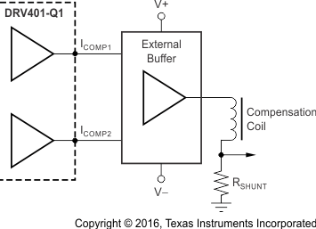 Figure 40. DRV401-Q1 with External Compensation Coil Driver and RSHUNT Connected to GND
7.3.5 Shunt Sense Amplifier
The differential (H-bridge) driver arrangement for the compensation coil requires a differential sense amplifier for the shunt voltage. This differential amplifier offers wide bandwidth and a high slew rate for fast current sensors. Excellent dc stability and accuracy result from an auto-zero technique. The voltage gain is 4 V/V, set by precisely matched and stable internal SiCr resistors.
7.3.6 Over-Range Comparator
High peak current can overload the differential amplifier connected to the shunt. The OVER-RANGE pin, an open-drain output, indicates an over-voltage condition for the differential amplifier by pulling low. The output of this flag is suppressed for 3 μs, preventing unwanted triggering from transients and noise. This pin returns to high when the overload condition is removed (an external pull-up is required to return the pin high).
This ERROR flag provides a warning about a signal clipping condition, but is also a window comparator output for actively shutting off circuits in the system. The value of the shunt resistor defines the operating window for the current. The value of the shunt resistor sets the ratio between the nominal signal and the trip level of the over-range flag. The trip current of this window comparator is calculated using the following example:
With a 5-V supply, the output voltage swing is approximately ±2.45 V (load and supply voltage-dependent).
The gain of 4 V/V allows an input swing of ±0.6125 V.
Thus, the clipping current is IMAX = 0.6125 V / RSHUNT.
See Figure 10.
The over-range condition is internally detected when the amplifier exceeds the linear operating range, not merely as a set voltage level. Therefore, the error or the over-range comparator level is reliably indicated in fault conditions such as output shorts, low load or low supply conditions. The flag is activated when the output cannot drive the voltage higher. The configuration is a safety improvement over a voltage level comparator.
NOTE
The internal resistance of the compensation coil may prevent high compensation current from flowing because of ICOMP driver overload. Therefore, the differential amplifier may not overload with this current. However, a fast rate of change of the primary current would be transmitted through transformer action and safely trigger the overload flag.
7.3.7 Voltage Reference
The precision 2.5-V reference circuit offers low drift (typically 10 ppm/K), used for internal biasing, and connects to the REFOUT pin. The circuit is intended as the reference point of the output signal to allow a bipolar signal around it. The output is buffered for low impedance and tolerates sink and source currents of ±5 mA. Capacitive loads may be directly connected, but generate ringing on fast load transients. A small series resistor of a few ohms improves the response, especially for a capacitive load in the range of 1 μF. Figure 41 illustrates this circuit configuration and the transient load regulation with 1-nF direct load.
The reference source is part of the integrated circuit and referenced to GND2. Large current pulses driving the compensation coil generates a voltage drop in the GND connection that may add on to the reference voltage. Therefore, a low impedance GND layout is critical to handle the currents and the high bandwidth of the device.
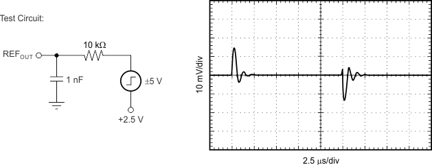 Figure 41. Pulse Response: Test Circuit and Scope Shot of Reference
7.3.8 Demagnetization
Iron cores are not immune to residual (remanence) magnetism. The residual remanence produces a signal offset error, especially after strong current overload, which goes along with high magnetic field density. Therefore, the DRV401-Q1 device includes a signal generator for a demagnetization cycle. The digital control pin, DEMAG, starts the cycle on demand after the pin is held high for at least 25.6 μs. Shorter pulses are ignored. The cycle lasts for approximately 110 ms. During this time, the ERROR flag is asserted low to indicate that the output is not valid. When DEMAG is high during power-on, a demagnetization cycle immediately initiates (12 μs) after power-on (VDD > 4 V). Holding DEMAG low avoids this cycle at power-up. See the Power-On and Brownout section for more information.
The probe circuit is in normal operation and oscillates during the demagnetization cycle. The PWM and PWM outputs are active accordingly.
A demagnetization cycle can be aborted by pulling DEMAG low, filtered by 25 μs to ignore glitches, as shown in Figure 46. In a typical circuit, the DEMAG pin may be connected to the positive supply, which enables a degauss cycle every time the unit is powered on.
The degauss cycle is based on an internal clock and counter logic. The maximum current is limited by the resistance of the connected coil in series with the shunt resistor. The DEMAG logic input requires a 5-V, CMOS-compatible signal.
7.3.9 Power-On and Brownout
Power-on is detected with the supply voltage going higher than 4 V at VDD1. When DEMAG is high, a degauss cycle is started, as shown in Figure 46 through Figure 49. During this time the ERROR flag remains low, indicating the not ready condition. Maintaining DEMAG low prevents this cycle, and the DRV401-Q1 device starts operation approximately 32 μs after power-up. If no probe error conditions are detected within four full cycles (that is, the probe half-periods are shorter than 32 μs and longer than 280 ns), the compensation driver starts and the ERROR pin indicates the ready condition by going high, typically about 42 μs after power-up.
NOTE
An external pull-up resistor is required to pull the ERROR pin high.
Both supply pins (VDD1 and VDD2) must not differ by more than 100 mV for proper device operation. They are normally connected together or separately filtered as shown in Layout.
The DRV401-Q1 device tests for low supply voltage with a brownout voltage level of 4 V; proper power conditions must be supplied. Good power-supply and low equivalent series resistance (ESR) bypass capacitors are required to maintain the supply voltage during the large current pulses that the DRV401-Q1 device drives.
A critical voltage level is derived from the proper operation of the probe driver. The probe interface relies on a peak current flowing through the probe to trip the comparator. The probe resistance plus the internal resistance of the driver (see Probe Coil Loop, Internal Resistor parameters in the Electrical Characteristics table) sets the lower limit for the acceptable supply voltage. Voltage drops lasting less than 31 μs are ignored. The probe error detection activates the ERROR pin when proper oscillation fails for more than 32 μs.
A low supply voltage condition, or brownout, is detected at 4 V. Short and light voltage drops of less than 100 μs are ignored, provided the probe circuit continues to operate. If the probe no longer operates, the ERROR pin goes active. Signal overload recovery is only provided if the probe loop was not discontinued.
A supply drop lasting longer than 100 μs generates power-on reset. A voltage dip down to 1.8 V (for VDD1) initiates a power-on reset.
7.3.10 Error Conditions
In addition to the overrange flag that indicates signal clipping in the output amplifier (differential amplifier), a system error flag is provided. The ERROR flag indicates conditions when the output voltage does not represent the primary current. The ERROR flag is active during a demagnetization cycle, power-fail, or brownout. The ERROR flag becomes active with an open or short-circuit in the probe loop. When the error condition is no longer present and the circuit returns to normal operation, the flag resets.
The ERROR and overrange flags are open-drain logic outputs. The flags connect together for a wired-OR and require an external pull-up resistor for proper operation.
The following conditions result in ERROR flag activation (ERROR asserts low):
- The probe comparator stays low for more than 32 μs. This condition occurs if the probe coil connection is open or if the supply voltage dips to the level where the required saturation current cannot be reached. During the 32-μs timeout, the ICOMP driver remains active but goes inactive thereafter. In case of recovery, ERROR is low and the ICOMP driver remains in reset for another 3.3 ms.
- The probe driver pulse-width is less than 280 ns for three consecutive periods. This condition indicates a shorted field probe coil or a fully-saturated sensor at start-up. If this condition persists longer than 25 μs and then recovers, the ERROR flag remains low and ICOMP is in reset for another 3.3 ms. If the condition lasts less than 25 μs, the ERROR flag recovers immediately and the ICOMP driver is not interrupted.
- During demagnetization, if the cycle is aborted early by pulling DEMAG low, the ERROR flag stays low for another 3.3 ms (ICOMP is disabled during this time).
- An open compensation coil is detected (longer than 100 μs). This condition indicates that not enough current is flowing in the ICOMP driver output; this condition may be the result of a high-resistance compensation coil or the connection of an external driver. Detection of this condition can be disabled by setting the CCdiag pin low.
- At power-on after VDD1 crosses the 4-V threshold, the ERROR flag is low for approximately 42 μs.
- A supply voltage low (brownout) condition lasts longer than 100 μs. Recovery is the same as power-up, with or without a demagnetization cycle.
NOTE
The probe driver, the PWM signal filter, and the ICOMP driver continue to function in normal mode. Only the ERROR flag is asserted in the case when an open compensation coil is detected.
7.3.11 Protection Recommendations
The IAIN1 and IAIN2 inputs require external protection to limit the voltage swing beyond 10 V of the supply voltage. The driver outputs ICOMP1 and ICOMP2 handles high current pulses protected by internal clamp circuits to the supply voltage. If repeated overcurrents of large magnitudes are expected, connect external Schottky diodes to the supply rails. This external protection prevents current flowing into the die.
The IS1 and IS2 probe connections are protected with diode clamps to the supply rails. In normal applications, no external protection is required. The maximum current must be limited to ±75 mA.
All other pins offer standard protection. See the Absolute Maximum Ratings table for more information.
7.4 Device Functional Modes
The DRV401-Q1 has a single functional mode and is operational when the power supply voltages, VDD1 and VDD2, are between 4.5 V and 5.5 V. For unusual operating conditions where a brownout condition may occur the DRV401-Q1 may perform a power-on reset. See the Power-On and Brownout section for a complete description of operation during a brownout.