SBOS814 December 2016 DRV401-Q1
PRODUCTION DATA.
- 1 Features
- 2 Applications
- 3 Description
- 4 Revision History
- 5 Pin Configuration and Functions
- 6 Specifications
-
7 Detailed Description
- 7.1 Overview
- 7.2 Functional Block Diagram
- 7.3
Feature Description
- 7.3.1 Magnetic Probe (Sensor) Interface
- 7.3.2 PWM Processing
- 7.3.3 Compensation Driver
- 7.3.4 External Compensation Coil Driver
- 7.3.5 Shunt Sense Amplifier
- 7.3.6 Over-Range Comparator
- 7.3.7 Voltage Reference
- 7.3.8 Demagnetization
- 7.3.9 Power-On and Brownout
- 7.3.10 Error Conditions
- 7.3.11 Protection Recommendations
- 7.4 Device Functional Modes
- 8 Application and Implementation
- 9 Power Supply Recommendations
- 10Layout
- 11Device and Documentation Support
- 12Mechanical, Packaging, and Orderable Information
Package Options
Mechanical Data (Package|Pins)
- RGW|20
Thermal pad, mechanical data (Package|Pins)
- RGW|20
Orderable Information
9 Power Supply Recommendations
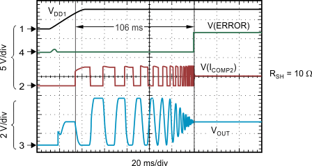
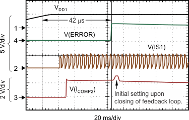
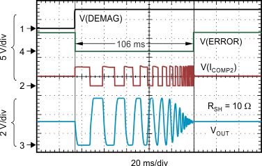
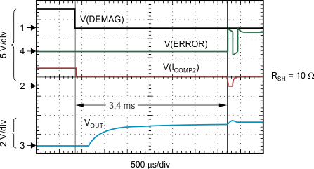
The DRV401-Q operates from a single power supply, nominally 5 V, and must remain between 4.5 V and 5.5 V for normal operation. See Figure 46, Figure 47, Figure 48, and Figure 49 for device power-on behavior.

With power-up, the VOUT across the compensation coil centers around half the supply and then starts the cycle after the 4-V threshold is exceeded. The ERROR flag resets to H after the cycle is completed.
Figure 46. Demagnetization and Power-On Timing: Demagnetization Cycle on Power-Up

The probe oscillation V(IS1) starts just before ERROR resets—15 μs after the supply voltage crosses the 4-V threshold.
Figure 47. Demagnetization and Power-On Timing: Power-Up Without Demagnetization
 Figure 48. Demagnetization and Power-On Timing: Demagnetization Cycle On Command

The ERROR flag resets to H (as shown) and the output settles back to normal operation.
Figure 49. Demagnetization and Power-On Timing: Abort of Demagnetization Cycle