SBAS914 February 2019 DRV5021-Q1
PRODUCTION DATA.
- 1 Features
- 2 Applications
- 3 Description
- 4 Revision History
- 5 Pin Configuration and Functions
- 6 Specifications
- 7 Detailed Description
- 8 Application and Implementation
- 9 Power Supply Recommendations
- 10Layout
- 11Device and Documentation Support
- 12Mechanical, Packaging, and Orderable Information
Package Options
Mechanical Data (Package|Pins)
- DBZ|3
Thermal pad, mechanical data (Package|Pins)
Orderable Information
7.3.5 Propagation Delay
The DRV5021-Q1 samples the Hall element at a nominal sampling period of 16.67 µs to detect the presence of a magnetic north or south pole. At each sampling point, the device takes the average of the current sampled value and immediately preceding sampled value of the magnetic field. If this average value crosses the BOP or BRP threshold, the device output changes according to the transfer function.
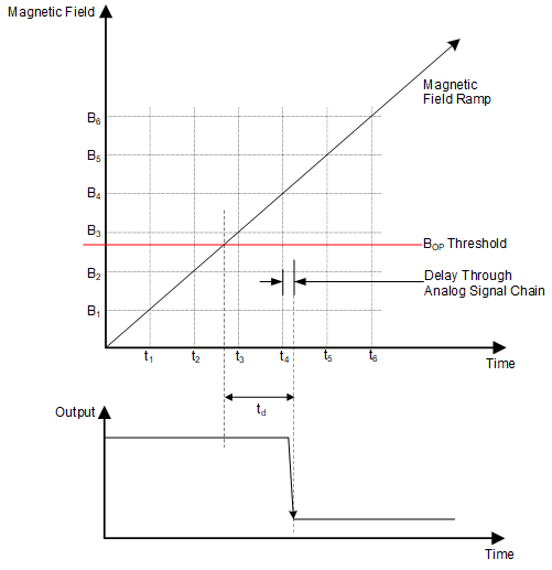
Figure 18 shows the DRV5021-Q1 propagation delay analysis in the proximity of a magnetic south pole. The Hall element of the DRV5021-Q1 experiences an increasing magnetic field as the magnetic south pole approaches near the device. At time t2, the average magnetic field is (B2 + B1) / 2, which is less than the BOP threshold of the device. At time t3, the actual magnetic field has crossed the BOP threshold. However, the average (B3 + B2) / 2 is still less than the BOP threshold. Thus, the device waits for next sample time, t4, to start the output transition through the analog signal chain. The propagation delay, td, is measured as the delay from the time the magnetic field crosses the BOP threshold to the time output transitions.
 Figure 18. Propagation Delay