SBAS913 December   2018 DRV5021

PRODUCTION DATA.  

  1. Features
  2. Applications
  3. Description
    1.     Device Images
      1.      Typical Application Schematic
      2.      Magnetic Response
  4. Revision History
  5. Pin Configuration and Functions
    1.     Pin Functions
  6. Specifications
    1. 6.1 Absolute Maximum Ratings
    2. 6.2 ESD Ratings
    3. 6.3 Recommended Operating Conditions
    4. 6.4 Thermal Information
    5. 6.5 Electrical Characteristics
    6. 6.6 Magnetic Characteristics
    7. 6.7 Typical Characteristics
  7. Detailed Description
    1. 7.1 Overview
    2. 7.2 Functional Block Diagram
    3. 7.3 Feature Description
      1. 7.3.1 Field Direction Definition
      2. 7.3.2 Device Output
      3. 7.3.3 Power-On Time
      4. 7.3.4 Hall Element Location
      5. 7.3.5 Propagation Delay
      6. 7.3.6 Output Stage
    4. 7.4 Device Functional Modes
  8. Application and Implementation
    1. 8.1 Application Information
    2. 8.2 Typical Applications
      1. 8.2.1 Proximity Sensing Circuit
        1. 8.2.1.1 Design Requirements
        2. 8.2.1.2 Detailed Design Procedure
          1. 8.2.1.2.1 Configuration Example
        3. 8.2.1.3 Application Curves
      2. 8.2.2 Alternative Two-Wire Application
        1. 8.2.2.1 Design Requirements
        2. 8.2.2.2 Detailed Design Procedure
  9. Power Supply Recommendations
  10. 10Layout
    1. 10.1 Layout Guidelines
    2. 10.2 Layout Example
  11. 11Device and Documentation Support
    1. 11.1 Documentation Support
      1. 11.1.1 Related Documentation
    2. 11.2 Receiving Notification of Documentation Updates
    3. 11.3 Community Resources
    4. 11.4 Trademarks
    5. 11.5 Electrostatic Discharge Caution
    6. 11.6 Glossary
  12. 12Mechanical, Packaging, and Orderable Information

Package Options

Mechanical Data (Package|Pins)
Thermal pad, mechanical data (Package|Pins)
Orderable Information

Application Curves

DRV5021 scope_1_slis151.gif
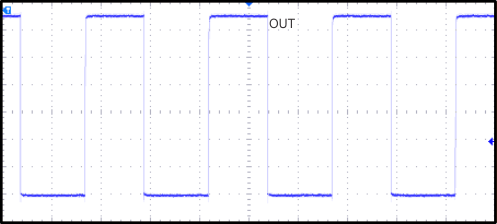
R1 = 10-kΩ pullup resistor, no C2 capacitor
Figure 21. 10-kHz Switching Magnetic Field
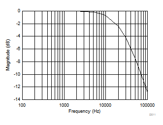
DRV5021 D011_SLIS150.gif
R1 = 10-kΩ pullup resistor, C2 = 680 pF
Figure 23. Low-Pass Filtering
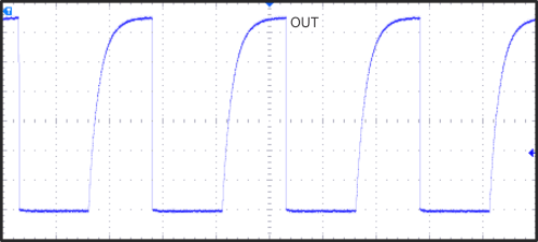
DRV5021 scope_2_slis151.gif
R1 = 10-kΩ pullup, C2 = 680 pF
Figure 22. 10-kHz Switching Magnetic Field