SBAS913 December 2018 DRV5021
PRODUCTION DATA.
- 1 Features
- 2 Applications
- 3 Description
- 4 Revision History
- 5 Pin Configuration and Functions
- 6 Specifications
- 7 Detailed Description
- 8 Application and Implementation
- 9 Power Supply Recommendations
- 10Layout
- 11Device and Documentation Support
- 12Mechanical, Packaging, and Orderable Information
Package Options
Mechanical Data (Package|Pins)
- DBZ|3
Thermal pad, mechanical data (Package|Pins)
Orderable Information
7.3.3 Power-On Time
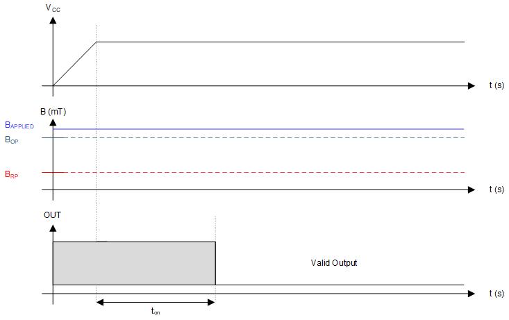
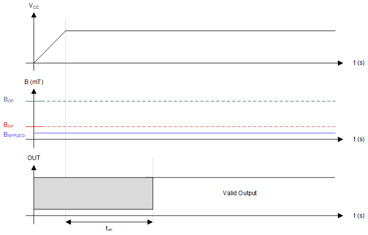
After applying VCC to the DRV5021, ton must elapse before the OUT pin is valid. In case 1 (Figure 13) and case 2 (Figure 14), the output is defined assuming that magnetic field BAPPLIED > BOP, and BAPPLIED < BRP, respectively.
 Figure 13. Case 1: Power On When B > BOP
  Figure 14. Case 2: Power On When B < BRP
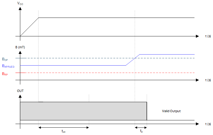
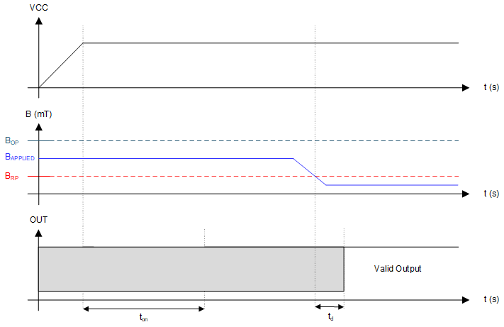
 If the device is powered on with BRP < BAPPLIED < BOP, then the device output remains in indeterminate state until the magnetic field changes. After the change in magnetic field results in a condition that meets either BOP < BAPPLIED or BRP > BAPPLIED, the output turns to valid state after td time elapses. Case 3 (Figure 15) and case 4 (Figure 16) show examples of this behavior.
 Figure 15. Case 3: Power On When BRP < B < BOP, Followed by B > BOP
  Figure 16. Case 4: Power On When BRP < B < BOP, Followed by B < BRP