SLVSCX2B August 2015 – February 2016 DRV8305
PRODUCTION DATA.
- 1 Features
- 2 Applications
- 3 Description
- 4 Revision History
- 5 Pin Configuration and Functions
- 6 Specifications
-
7 Detailed Description
- 7.1 Overview
- 7.2 Functional Block Diagram
- 7.3
Feature Description
- 7.3.1 Integrated Three-Phase Gate Driver
- 7.3.2 INHx/INLx: Gate Driver Input Modes
- 7.3.3 VCPH Charge Pump: High-Side Gate Supply
- 7.3.4 VCP_LSD LDO: Low-Side Gate Supply
- 7.3.5 GHx/GLx: Half-Bridge Gate Drivers
- 7.3.6 DVDD and AVDD: Internal Voltage Regulators
- 7.3.7 VREG: Voltage Regulator Output
- 7.3.8 Protection Features
- 7.3.9 Undervoltage Warning (UVFL), Undervoltage Lockout (UVLO), and Overvoltage (OV) Protection
- 7.4 Device Functional Modes
- 7.5 Programming
- 7.6
Register Maps
- 7.6.1 Status Registers
- 7.6.2
Control Registers
- 7.6.2.1 HS Gate Drive Control (Address = 0x5)
- 7.6.2.2 LS Gate Drive Control (Address = 0x6)
- 7.6.2.3 Gate Drive Control (Address = 0x7)
- 7.6.2.4 IC Operation (Address = 0x9)
- 7.6.2.5 Shunt Amplifier Control (Address = 0xA)
- 7.6.2.6 Voltage Regulator Control (Address = 0xB)
- 7.6.2.7 VDS Sense Control (Address = 0xC)
- 8 Application and Implementation
- 9 Power Supply Recommendations
- 10Layout
- 11Device and Documentation Support
- 12Mechanical, Packaging, and Orderable Information
Package Options
Mechanical Data (Package|Pins)
- PHP|48
Thermal pad, mechanical data (Package|Pins)
- PHP|48
Orderable Information
8 Application and Implementation
NOTE
Information in the following applications sections is not part of the TI component specification, and TI does not warrant its accuracy or completeness. TI’s customers are responsible for determining suitability of components for their purposes. Customers should validate and test their design implementation to confirm system functionality.
8.1 Application Information
The DRV8305 is a gate driver IC designed to drive a 3-phase BLDC motor in combination with external power MOSFETs. The device provides a high level of integration with three half-bridge gate drivers, three current shunt amplifiers, adjustable slew rate control, logic LDO, and a suite of protection features.
8.2 Typical Application
The following design is a common application of the DRV8305.
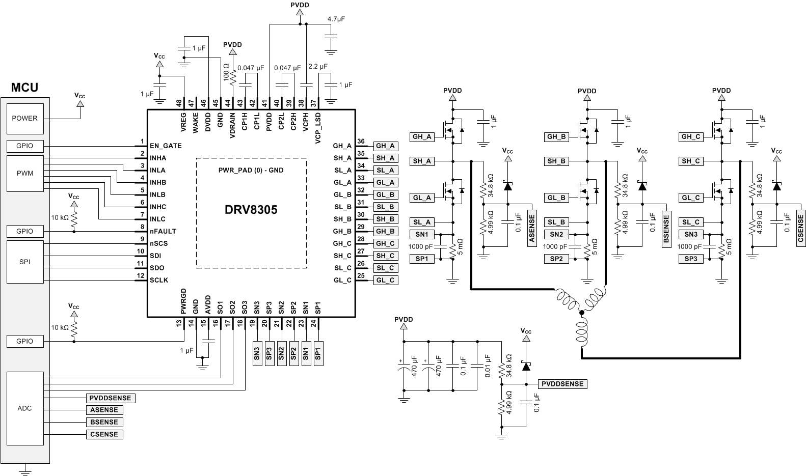 Figure 18. Typical Application Schematic
8.2.1 Design Requirements
Table 20. Design Parameters
| DESIGN PARAMETER | REFERENCE | VALUE |
|---|---|---|
| Supply voltage | PVDD | 12 V |
| Motor winding resistance | MR | 0.5 Ω |
| Motor winding inductance | ML | 0.28 mH |
| Motor poles | MP | 16 poles |
| Motor rated RPM | MRPM | 2000 RPM |
| Number of MOSFETs switching | NSW | 6 |
| Switching frequency | fSW | 45 kHz |
| IDRIVEP | IDRIVEP | 50 mA |
| IDRIVEN | IDRIVEN | 60 mA |
| MOSFET QG | Qg | 36 nC |
| MOSFET QGD | QGD | 9 nC |
| MOSFET RDS(on) | RDS(on) | 4.1 mΩ |
| Target full-scale current | IMAX | 30 A |
| Sense resistor | RSENSE | 0.005 Ω |
| VDS trip level | VDS_LVL | 0.197 V |
| Amplifier bias | VBIAS | 1.65 V |
| Amplifier gain | Gain | 10 V/V |
8.2.2 Detailed Design Procedure
8.2.2.1 Gate Drive Average Current
The gate drive supply (VCP) of the DRV8305 is capable of delivering up to 30 mA (RMS) of current to the external power MOSFETs. The charge pump directly supplies the high-side N-channel MOSFETs and a 10-V LDO powered from VCP supplies the low-side N-channel MOSFETs. The designer can determine the approximate RMS load on the gate drive supply through the following equation.
Example: 36 nC (QG) × 6 (NSW) × 45 kHz (fSW) = 9.72 mA
Note that this is only a first-order approximation.
8.2.2.2 MOSFET Slew Rates
The rise and fall times of the external power MOSFET can be adjusted through the use of the DRV8305 IDRIVE setting. A higher IDRIVE setting will charge the MOSFET gate more rapidly where a lower IDRIVE setting will charge the MOSFET gate more slowly. System testing requires fine tuning to the desired slew rate, but a rough first-order approximation can be calculated as shown in the following.
Example: 9 nC (QGD) / 50 mA (IDRIVEP) = 180 ns
8.2.2.3 Overcurrent Protection
The DRV8305 provides overcurrent protection for the external power MOSFETs through the use of VDS monitors for both the high-side and low-side MOSFETs. These are intended for protecting the MOSFET in overcurrent conditions and are not for precise current regulation.
The overcurrent protection works by monitoring the VDS voltage drop of the external MOSFETs and comparing it against the internal VDS_LEVEL set through the SPI registers. The high-side VDS is measured across the VDRAIN and SH_X pins. The low-side VDS is measured across the SH_X and SL_X pins. If the VDS voltage exceeds the VDS_LEVEL value, the DRV8305 will take action according to the VDS_MODE register.
The overcurrent trip level can be determined with the MOSFET RDS(on) and the VDS_LEVEL setting.
Example: 0.197 V (VDS_LVL) / 4.1 mΩ (RDS(ON)) = 48 A
8.2.2.4 Current Sense Amplifiers
The DRV8305 provides three bidirectional low-side current shunt amplifiers. These can be used to sense the current flowing through each half-bridge. If individual half-bridge sensing is not required, a single current shunt amplifier can be used to measure the sum of the half-bridge current. Use this simple procedure to correctly configure the current shunt amplifiers.
- Determine the peak current that the motor will demand (IMAX). This demand depends on the motor parameters and the application requirements. IMAX in this example is 14 A.
- Determine the available voltage output range for the current shunt amplifiers. This will be the ± voltage around the amplifier bias voltage (VBIAS). In this case VBIAS = 1.65 V and a valid output voltage is 0 to 3.3 V. This gives an output range of ±1.65 V.
- Determine the sense resistor value and amplifier gain settings. The sense resistor value and amplifier gain have common tradeoffs. The larger the sense resistor value, the better the resolution of the half-bridge current. This comes at the cost of additional power dissipated from the sense resistor. A larger gain value allows for the use of a smaller resolution, but at the cost of increased noise in the output signal and a longer settling time. This example uses a 5-mΩ sense resistor and the minimum gain setting of the DRV8305 (10 V/V). These values allow the current shunt amplifiers to measure ±33 A across the sense resistor.
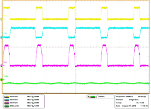
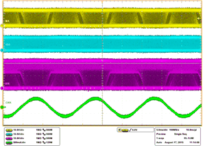
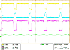
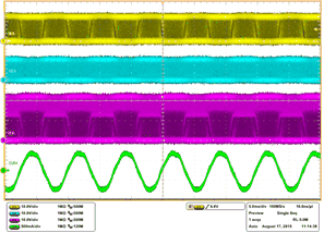
8.2.3 Application Curves
