SLVSCX2B August 2015 – February 2016 DRV8305
PRODUCTION DATA.
- 1 Features
- 2 Applications
- 3 Description
- 4 Revision History
- 5 Pin Configuration and Functions
- 6 Specifications
-
7 Detailed Description
- 7.1 Overview
- 7.2 Functional Block Diagram
- 7.3
Feature Description
- 7.3.1 Integrated Three-Phase Gate Driver
- 7.3.2 INHx/INLx: Gate Driver Input Modes
- 7.3.3 VCPH Charge Pump: High-Side Gate Supply
- 7.3.4 VCP_LSD LDO: Low-Side Gate Supply
- 7.3.5 GHx/GLx: Half-Bridge Gate Drivers
- 7.3.6 DVDD and AVDD: Internal Voltage Regulators
- 7.3.7 VREG: Voltage Regulator Output
- 7.3.8 Protection Features
- 7.3.9 Undervoltage Warning (UVFL), Undervoltage Lockout (UVLO), and Overvoltage (OV) Protection
- 7.4 Device Functional Modes
- 7.5 Programming
- 7.6
Register Maps
- 7.6.1 Status Registers
- 7.6.2
Control Registers
- 7.6.2.1 HS Gate Drive Control (Address = 0x5)
- 7.6.2.2 LS Gate Drive Control (Address = 0x6)
- 7.6.2.3 Gate Drive Control (Address = 0x7)
- 7.6.2.4 IC Operation (Address = 0x9)
- 7.6.2.5 Shunt Amplifier Control (Address = 0xA)
- 7.6.2.6 Voltage Regulator Control (Address = 0xB)
- 7.6.2.7 VDS Sense Control (Address = 0xC)
- 8 Application and Implementation
- 9 Power Supply Recommendations
- 10Layout
- 11Device and Documentation Support
- 12Mechanical, Packaging, and Orderable Information
Package Options
Mechanical Data (Package|Pins)
- PHP|48
Thermal pad, mechanical data (Package|Pins)
- PHP|48
Orderable Information
7 Detailed Description
7.1 Overview
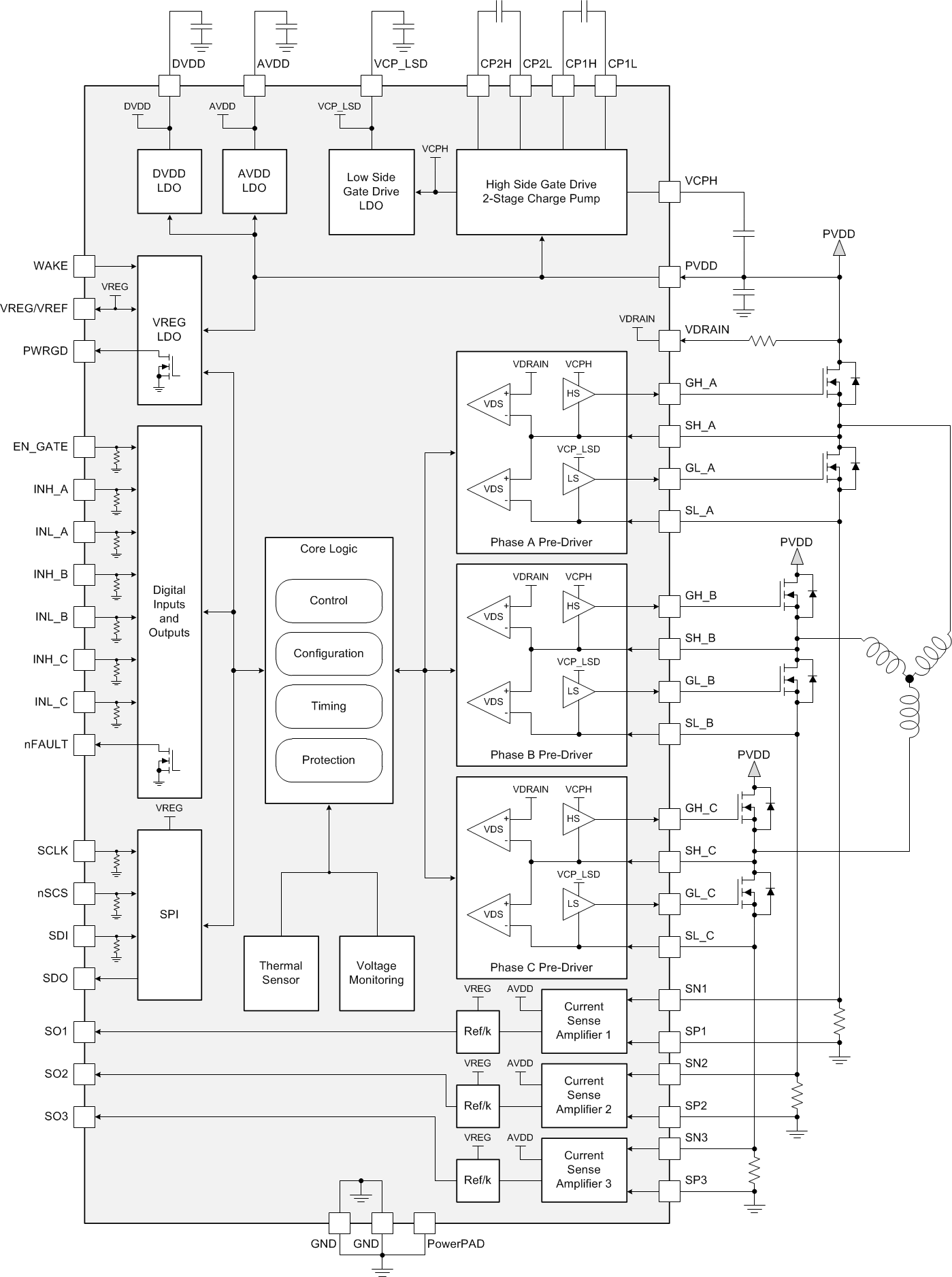
The DRV8305 is a 4.4-V to 45-V gate driver IC for three-phase motor driver applications. This device reduces external component count in the system by integrating three half-bridge drivers, charge pump, three current shunt amplifiers, an uncommited 3.3-V or 5-V, 50-mA LDO, and a variety of protection circuits. The DRV8305 provides overcurrent, shoot-through, overtemperature, overvoltage, and undervoltage protection. Fault conditions are indicated by the nFAULT pin and specific fault information can be read back from the SPI registers. The protection circuits are highly configurable to allow adaptation to different applications and support limp home operation.
The gate driver uses a tripler charge pump to generate the appropriate gate to source voltage bias for the external, high-side N-channel power MOSFETs during low supply conditions. A regulated 10-V LDO derived from the charge pump supplies the gate to source voltage bias for the low-side N-channel MOSFET. The high-side and low-side peak gate drive currents are adjustable through the SPI registers to finely tune the switching of the external MOSFETs without the need for external components. An internal handshaking scheme is used to prevent shoot-through and minimize the dead time when transitioning between MOSFETs in each half-bridge. Multiple input methods are provided to accommodate different control schemes including a 1-PWM mode which integrates a six-step block commutation table for BLDC motor control.
VDS sensing of the external power MOSFETs allows for the DRV8305 to detect overcurrent conditions and respond appropriately. Integrated blanking and deglitch timers are provided to prevent false trips related to switching or transient noise. Individual MOSFET overcurrent conditions are reported through the SPI status registers and nFAULT pin. A dedicated VDRAIN pin is provided to accurately sense the drain voltage of the high-side MOSFET.
The three internal current shunt amplifiers allow for the implementation of common motor control schemes that require sensing of the half-bridge currents through a low-side current shunt resistor. The amplifier gain, reference voltage, and blanking are adjustable through the SPI registers. A calibration method is providing to minimize inaccuracy related to offset voltage.
Three versions of the DRV8305 are available with separate part numbers for the different devices options:
- DRV8305N: VREG pin has the internal LDO disabled and is only used as a voltage reference input for the amplifiers and SDO pullup.
- DRV83053: VREG is a 3.3-V, 50-mA LDO output pin.
- DRV83055: VREG is a 5.0-V, 50-mA LDO output pin.
7.2 Functional Block Diagram
7.3 Feature Description
7.3.1 Integrated Three-Phase Gate Driver
The DRV8305 is a completely integrated three-phase gate driver. It provides three N-channel MOSFET half-bridge gate drivers, multiple input modes, high-side and low-side gate drive supplies, and a highly configurable gate drive architecture. The DRV8305 is designed to support a variety applications by incorporating a wide operating voltage range, wide temperature range, and array of protection features. The configurability of device allows for it to be used in a broad range of applications.
7.3.2 INHx/INLx: Gate Driver Input Modes
The DRV8305 can be operated in three different inputs modes to support various commutation schemes.
- Table 1 shows the truth table for the 6-PWM input mode. This mode allows for each half-bridge to be placed in one of three states, either High, Low, or Hi-Z, based on the inputs.
- Table 2 shows the truth table for the 3-PWM input mode. This mode allows for each half-bridge to be placed in one of two states, either High or Low, based on the inputs. The three high-side inputs (INHx) are used to control the state of the half-bridge with the complimentary low-side signals being generated internally. Deadtime can be adjusted through the internal setting (DEAD_TIME) in the SPI registers. In this mode all activity on INLx is ignored.
- Table 3 and Table 4 show the truth tables for the 1-PWM input mode. The 1-PWM mode uses an internally stored 6-step block commutation table to control the outputs of the three half-bridge drivers based on one PWM and three GPIO inputs. This mode allows the use of a lower cost microcontroller by requiring only one PWM resource. The PWM signal is applied on pin INHA (PWM_IN) to set the duty cycle of the half-bridge outputs along with the three GPIO signals on pins INLA (PHC_0), INHB (PHC_1), INLB (PHC_2) that serve to set the value of a three bit register for the commutation table. The PWM may be operated from 0-100% duty cycle. The three bit register is used to select the state for each half-bridge for a total of eight states including an align and stop state.
Table 1. 6-PWM Truth Table
| INHx | INLx | GHx | GLx |
|---|---|---|---|
| 1 | 1 | L | L |
| 1 | 0 | H | L |
| 0 | 1 | L | H |
| 0 | 0 | L | L |
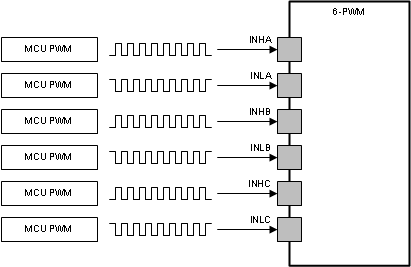 Figure 6. 6-PWM Mode
Table 2. 3-PWM Truth Table
| INHx | INLx | GHx | GLx |
|---|---|---|---|
| 1 | X | H | L |
| 0 | X | L | H |
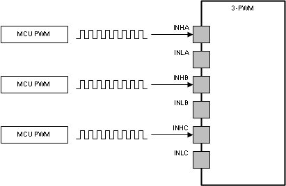 Figure 7. 3-PWM Mode
An additional and optional GPIO, INHC (DWELL) can be used to facilitate the insertion of dwell states or phase current overlap states between the six commutation steps. This may be used to reduce acoustic noise and improve motion through the reduction of abrupt current direction changes when switching between states. INHC must be high when the state is changed and the dwell state will exist until INHC is taken low. If the dwell states are not being used, the INHC pin can be tied low.
In 1-PWM mode all activity on INLC is ignored.
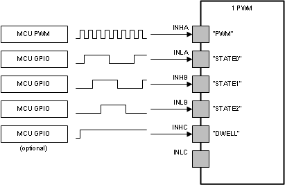 Figure 8. 1-PWM Mode
The method of freewheeling can be selected through an SPI register (COMM_OPTION). Diode freewheeling is when the phase current is carried by the body diode of the external power MOSFET during periods when the MOSFET is reverse biased (current moving from source to drain). In active freewheeling, the power MOSFET is enabled during periods when the MOSFET is reverse biased. This allows the system to improve efficiency due to the typically lower impedance of the MOSFET conduction channel as compared to the body diode. Table 3 shows the truth table for active freewheeling. Table 4 shows the truth table for diode freewheeling.
Table 3. 1-PWM Active Freewheeling
| STATE | INLA:INHB:INLB:INHC | GHA | GLA | GHB | GLB | GHC | GLC |
|---|---|---|---|---|---|---|---|
| AB | 0110 | PWM | !PWM | LOW | HIGH | LOW | LOW |
| AB_CB | 0101 | PWM | !PWM | LOW | HIGH | PWM | !PWM |
| CB | 0100 | LOW | LOW | LOW | HIGH | PWM | !PWM |
| CB_CA | 1101 | LOW | HIGH | LOW | HIGH | PWM | !PWM |
| CA | 1100 | LOW | HIGH | LOW | LOW | PWM | !PWM |
| CA_BA | 1001 | LOW | HIGH | PWM | !PWM | PWM | !PWM |
| BA | 1000 | LOW | HIGH | PWM | !PWM | LOW | LOW |
| BA_BC | 1011 | LOW | HIGH | PWM | !PWM | LOW | HIGH |
| BC | 1010 | LOW | LOW | PWM | !PWM | LOW | HIGH |
| BC_AC | 0011 | PWM | !PWM | PWM | !PWM | LOW | HIGH |
| AC | 0010 | PWM | !PWM | LOW | LOW | LOW | HIGH |
| AC_AB | 0111 | PWM | !PWM | LOW | HIGH | LOW | HIGH |
| Align | 1110 | PWM | !PWM | LOW | HIGH | LOW | HIGH |
| Stop | 0000 | LOW | LOW | LOW | LOW | LOW | LOW |
Table 4. 1-PWM Diode Freewheeling
| STATE | INLA:INHB:INLB:INHC | GHA | GLA | GHB | GLB | GHC | GLC |
|---|---|---|---|---|---|---|---|
| AB | 0110 | PWM | LOW | LOW | HIGH | LOW | LOW |
| AB_CB | 0101 | PWM | LOW | LOW | HIGH | PWM | LOW |
| CB | 0100 | LOW | LOW | LOW | HIGH | PWM | LOW |
| CB_CA | 1101 | LOW | HIGH | LOW | HIGH | PWM | LOW |
| CA | 1100 | LOW | HIGH | LOW | LOW | PWM | LOW |
| CA_BA | 1001 | LOW | HIGH | PWM | LOW | PWM | LOW |
| BA | 1000 | LOW | HIGH | PWM | LOW | LOW | LOW |
| BA_BC | 1011 | LOW | HIGH | PWM | LOW | LOW | HIGH |
| BC | 1010 | LOW | LOW | PWM | LOW | LOW | HIGH |
| BC_AC | 0011 | PWM | LOW | PWM | LOW | LOW | HIGH |
| AC | 0010 | PWM | LOW | LOW | LOW | LOW | HIGH |
| AC_AB | 0111 | PWM | LOW | LOW | HIGH | LOW | HIGH |
| Align | 1110 | PWM | LOW | LOW | HIGH | LOW | HIGH |
| Stop | 0000 | LOW | LOW | LOW | LOW | LOW | LOW |
7.3.3 VCPH Charge Pump: High-Side Gate Supply
The DRV8305 uses a charge pump to generate the proper gate to source voltage bias for the high-side N-channel MOSFETs. Similar to the often used bootstrap architecture, the charge pump generates a floating supply voltage used to enable the MOSFET. When enabled, the gate of the external MOSFET is connected to VCPH through the internal gate drivers. The charge pump of the DRV8305 regulates the VCPH supply to PVDD + 10-V in order to support both standard and logic level MOSFETs. As opposed to a bootstrap architecture, the charge pump supports 0 to 100% duty cycle operation by eliminating the need to refresh the bootstrap capacitor. The charge pump also removes the need for bootstrap capacitors to be connected to the switch-node of the half-bridge.
To support low-voltage operation, a regulated triple charge pump scheme is used to create sufficient VGS to drive standard and logic level MOSFETs during the low voltage transient. Between 4.4 to 18 V the charge pump regulates the voltage in a tripler mode. Beyond 18 V and until the max operating voltage, it switches over to a doubler mode in order to improve efficiency. The charge pump is disabled until EN_GATE is set high to reduce unneeded power consumption by the IC. After EN_GATE is set high, the device will go through a power up sequence to enable the gate drivers and gate drive supplies. 1 ms should be allocated after EN_GATE is set high to allow the charge pump to reach its regulation voltage.
The charge pump is continuously monitored for undervoltage and overvoltage conditions to prevent underdriven or overdriven MOSFET scenarios. If an undervoltage or overvoltage condition is detected the appropriate actions is taken and reported through the SPI registers.
7.3.4 VCP_LSD LDO: Low-Side Gate Supply
The DRV8305 uses a linear regulator to generate the proper gate to source voltage vias for the low-side N-channel MOSFETs. The linear regulator generates a fixed 10-V supply voltage with respect to GND. When enabled, the gate of the external MOSFET is connected to VCPH_LSD through the internal gate drivers. To support low-voltage operation, the input voltage for the VCP_LSD linear regulator is taken from the VCPH charge pump. This allows the DRV8305 to provide sufficient VGS to drive standard and logic level MOSFETs during the low voltage transient.
The low-side regulator is disabled until EN_GATE is set high to reduce unneeded power consumption by the IC. After EN_GATE is set high, the device will go through a power up sequence for the gate drivers and gate drive supplies. 1 ms should be allocated after EN_GATE is set high to allow the low-side regulator to reach its regulation voltage. The VCP_LSD regulator is continuously monitored for undervoltage conditions to prevent underdriven MOSFET scenarios. If an undervoltage condition is detected the appropriate actions is taken and reported through the SPI registers.
7.3.5 GHx/GLx: Half-Bridge Gate Drivers
The DRV8305 gate driver uses a complimentary push-pull topology for both the high-side and the low-side gate drivers. Both the high-side (GHx to SHx) and the low-side (GLx to SLx) are implemented as floating gate drivers in order to tolerate switching transients from the half-bridges. The high-side and low-side gate drivers use a highly adjustable current control scheme in order to allow the DRV8305 to adjust the VDS slew rate of the external MOSFETs without the need for additional components. The scheme also incorporates a mechanism for detecting issues with the gate drive output to the power MOSFETs during operation. This scheme and its application benefits are outlined below as well as in application report, SLVA714.
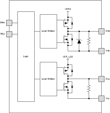 Figure 9. DRV8305 Gate Driver Architecture
7.3.5.1 IDRIVE: Gate Driver Output Current
The first component of the gate drive architecture implements adjustable current control for the gates of the external power MOSFETs. This feature allows the gate driver to control the VDS slew rate of the MOSFETs by adjusting the gate drive current. This is realized internally to reduce the need for external components inline with the gates of the MOSFETs. The DRV8305 provides 12 adjustable source and sink current levels for the high-side (the high sides of all three phases share the same setting) and low-side gate drivers (the low sides of all three phases share the same settings). The gate drive levels are adjustable through the SPI registers in both the standby and operating states. This flexibility allows the system designer to tune the performance of the driver for different operating conditions through software alone.
The gate drivers are implemented as temperature compensated, constant current sources up to the 80 mA (sink)/70 mA (source) current settings in order to maintain the accuracy required for precise slew rate control. The current source architecture helps eliminate the temperature, process, and load-dependent variation associated with internal and external series limiting resistors. Beyond that, internal switches are adjusted to create the desired settings up to the 1.25 A (sink)/1 A (source) settings. For higher currents, internal series switches are used to minimize the power losses associated with mirroring such large currents.
Control of the gate current during the MOSFET Miller region is a key component for adjusting the MOSFET VDS rise and fall times. MOSFET VDS slew rates are a critical parameter for optimizing emitted radiations, energy and duration of diode recovery spikes, dV/dt related turn on leading to shoot-through, and voltage transients related to parasitics.
When a MOSFET is enhanced, three different charges must be supplied to the MOSFET gate. The MOSFET drain to source voltage will slew primarily during the Miller region. By controlling the rate of charge to the MOSFET gate (gate drive current strength) during the Miller region, it is possible to optimize the VDS slew rate for the reasons mentioned.
- QGS = Gate-to-source charge
- QGD = Gate-to-drain charge (Miller charge)
- Remaining QG
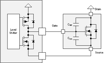 Figure 10. MOSFET Charge Example
7.3.5.2 TDRIVE: Gate Driver State Machine
The DRV8305 gate driver uses an integrated state machine (TDRIVE) in the gate driver to protect against excessive current on the gate drive outputs, shoot-through in the external MOSFET, and dV/dt turn on due to switching on the phase nodes. The TDRIVE state machine allows for the design of a robust and efficient motor drive system with minimal overhead.
The state machine incorporates internal handshaking when switching from the low to the high-side external MOSFET or vice-versa. The handshaking is designed to prevent the external MOSFETs from entering a period of cross conduction, also known as shoot-through. The internal handshaking uses the VGS monitors of the DRV8305 to determine when one MOSFET has been disabled and the other can be enabled. This allows the gate driver to insert an optimized dead time into the system without the risk of cross conduction. Any deadtime added externally through the MCU or SPI register will be inserted after the handshake process.
The state machine also incorporates a gate drive timer to ensure that under abnormal circumstances such as a short on the MOSFET gate or the inadvertent turn on of a MOSFET VGS clamp, the high peak current through the DRV8305 and MOSFET is limited to a fixed duration. This concept is visualized in the figure below. First, the DRV8305 receives a command to enable or disable the MOSFET through INHx or INLx inputs. Second, the gate driver is enabled and a strong current is applied to the MOSFET gate and the gate voltage begins to change. If the gate voltage has not changed to the desired level after the tDRIVE period (indicating a short circuit or overcurrent condition on the MOSFET gate), the DRV8305 signals a gate drive fault and the gate drive is disabled to help protect the external MOSFET and DRV8305. If the MOSFET does successfully enable or disable, after the tDRIVE period the DRV8305 will enable a lower hold current to ensure the MOSFET remains enabled or disabled and improve efficiency of the gate drive.
Select a tDRIVE time that is longer than the time needed to charge or discharge the gate capacitances of the external MOSFETs. The TDRIVE SPI registers should be configured so that the MOSFET gates are charged completely within tDRIVE during normal operation. If tDRIVE is too low for a given MOSFET, then the MOSFET may not turn on completely. It is suggested to tune these values in-system with the required external MOSFETs to determine the best possible setting for the application. A good starting value is a tDRIVE period that is 2x the expected rise or fall times of the external MOSFET gates. Note that TDRIVE will not increase the PWM time and will simply terminate if a PWM command is received while it is active.
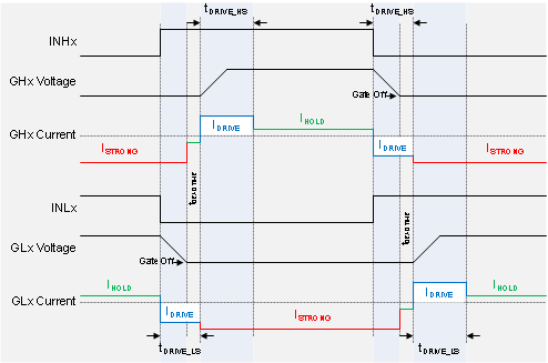 Figure 11. TDRIVE Gate Drive State Machine
7.3.5.3 CSAs: Current Shunt Amplifiers
The DRV8305 includes three high performance low-side current shunt amplifiers for accurate current measurement utilizing low-side shunt resistors in the external half-bridges. They are commonly used to measure the motor phase current to implement overcurrent protection, external torque control, or external commutation control through the application MCU.
The current shunt amplifiers have the following features:
- Each of the three current sense amplifiers can be programmed and calibrated independently.
- Can provide output bias up to 2.5 V to support bidirectional current sensing.
- May be used for either individual or total current shunt sensing.
- Four programmable gain settings through SPI registers (10, 20, 40 and 80 V/V).
- Reference voltage for output bias provided from voltage regulator VREG for DRV83053Q and DRV83055Q
- Reference voltage for output bias provided from externally applied voltage on VREG pin for DRV8305NQ and DRV8305NE
- Programmable output bias scaling. The scaling factor k can be programmed through SPI registers (1/2 or 1/4)
- Programmable blanking time (delay) of the amplifier outputs. The blanking time is implemented from any rising or falling edge of gate drive outputs. The blanking time is applied to all three current sense amplifiers equally. In case the current sense amplifiers are already being blanked when another gate driver rising or falling edge is seen, the blanking interval will be restarted at the edge. Note that the blanking time options do not include delay from internal amplifier loading or delays from the trace or component loads on the amplifier output. The programmable blanking time may be overridden to have no delay (default value).
- Minimize DC offset and drift through temperature with DC calibrating through SPI register. When DC calibration is enabled, device will short input of current shunt amplifier and disconnect the load. DC calibrating can be done at anytime, even when the MOSFET is switching because the load is disconnected. For best result, perform the DC calibrating during switching off period when no load is present to reduce the potential noise impact to the amplifier.
The output of current shunt amplifier can be calculated as:

where
- VREF is the reference voltage from the VREG pin.
- G is the gain setting of the amplifier.
- k = 2 or 4
- SNx and SPx are the inputs of channel x.
- SPx should connect to the low-side (ground) of the sense resistor for the best common mode rejection.
- SNx should connect to the high-side (LS MOSFET source) of the sense resistor.
Figure 12 shows current amplifier simplified block diagram.
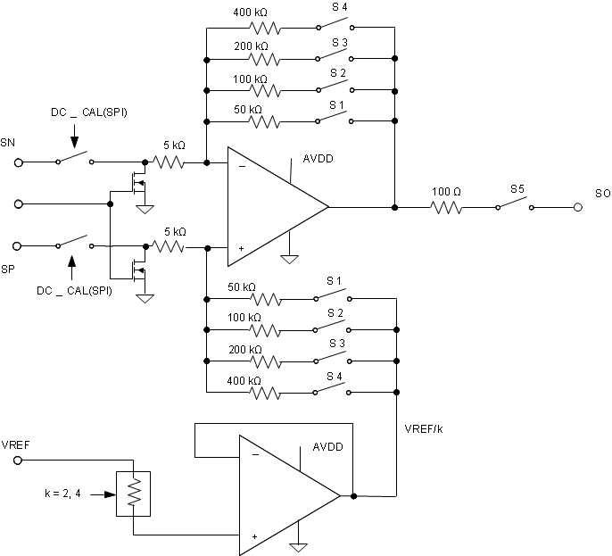 Figure 12. Current Shunt Amplifier Simplified Block Diagram
7.3.6 DVDD and AVDD: Internal Voltage Regulators
The DRV8305 has two internal regulators, DVDD and AVDD, that power internal circuitry. These regulators cannot be used to drive external loads and may not be supplied externally.
DVDD is the voltage regulator for the internal logic circuits and is maintained at a value of 3.3 V through the entire operating range of the device. DVDD is derived from the PVDD power supply. DVDD should be bypassed externally with a 1-µF capacitor to GND.
AVDD is the voltage regulator that provides the voltage rail for the internal analog circuit blocks including the current sense amplifiers and is maintained at a value 5 V. AVDD is derived from the PVDD voltage power supply. AVDD should be bypassed externally with a 1-µF capacitor to GND.
Because the allowed PVDD operating range of the device permits operation below the nominal value of AVDD, this regulator operates in two regimes: namely a linear regulating regime and a dropout region. In the dropout region, the AVDD will simply track the PVDD voltage minus a voltage drop.
If the device is expected to operate within the dropout region, take care while selecting current sense amplifier components and settings to accommodate the reduced voltage rail.
7.3.7 VREG: Voltage Regulator Output
The DRV8305 integrates a 50 mA, LDO voltage regulator (VREG) that is dedicated for driving external loads such as an MCU directly. The VREG regulator also supplies the reference for the SDO output of the SPI bus and the voltage reference for the amplifier output bias. The three different DRV8305 device versions provide different configurations for the VREG output. For the DRV83053Q, the VREG output is regulated at 3.3 V. For the DRV83055Q, the VREG output is regulated at 5 V. For the DRV8305NQ and DRV8305NE, the VREG voltage regulator is disabled (VREG pin used for reference voltage) and the reference voltage for SDO and the amplifier output bias must be supplied from an external supply to the VREG pin.
The DRV8305 VREG voltage regulator also features a PWRGD pin to protect against brownouts on externally driven devices. The PWRGD pin is often tied to the reset pin of a microcontroller to ensure that the microcontroller is always reset when the VREG output voltage is outside of its recommended operation area.
When the voltage output of the VREG regulator drops or exceeds the set threshold (programmable).
- The PWRGD pin will go low for a period of 56 µs.
- After the 56 µs period has expired, the VREG voltage will be checked and PWRGD will be held low until the VREG voltage has recovered.
The voltage regulator also has undervoltage protection implemented for both the input voltage (PVDD) and output voltage (VREG).
7.3.8 Protection Features
7.3.8.1 Fault and Warning Classification
The DRV8305 integrates extensive error detection and monitoring features. These features allow the design of a robust system that can protect against a variety of system related failure modes. The DRV8305 classifies error events into two categories and takes different device actions dependent on the error classification.
The first error class is a Warning. There are several types of conditions that are classified as warning only. Warning errors are report only and the DRV8305 will take no other action effecting the gate drivers or other blocks. When a warning condition occurs it will be reported in the corresponding SPI status register bit and on the nFAULT pin with a repeating 56 µs pulse low followed by a 56 µs pulse high. A warning error can be cleared by an SPI read to the corresponding status register bit. The same warning will not be reported through the nFAULT pin again unless that warning or condition passes and then reoccurs.
- A warning error is reported on the nFAULT pin with a repeating 56 µs pulse low followed by a 56 µs pulse high
- The warning is reported on the nFAULT pin until a SPI read to the corresponding status register
- The SPI read will clear the nFAULT report, but the SPI register will remain asserted until the condition has passed
- The nFAULT pin will report a new warning if the condition clears and then occurs again
The second error class is a Fault. Fault errors will trigger a shutdown of the gate driver with its major blocks and are reported by holding nFAULT low with the corresponding status register asserted. Fault errors are latched until the appropriate recovery sequence is performed.
- A fault error is reported by holding the nFAULT pin low and asserting the FAULT bit in register 0x1
- The error type will also be asserted in the SPI registers
- A fault error is a latched fault and must be cleared with the appropriate recovery sequence
- If a fault occurs during a warning error, the fault error will take precendence, latch nFAULT low and shutdown the gate driver
- The output MOSFETs will be placed into their high impedance state in a fault error event
- To recover from a fault type error, the condition must be removed and the CLR_FLTs bit asserted in register 0x9, bit D1 or an EN_GATE reset pulse issued
- The CLR_FLTS bit self clears to 0 after fault status reset and nFAULT pin is released
There are two exceptions to the fault and warning error classes. The first exception is the temperature flag warnings (TEMP_FLAGX). A Temperature Flag warning will not trigger any action on the nFAULT pin and the corresponding status bit will be updated in real time. See the overtemperature section for additional information. The second exception is the MCU Watchdog and VREG Undervoltage (VREG_UV) faults. These are reported on the PWRGD pin to protect the system from lock out and brownout conditions. See their corresponding sections for additional information.
Note that nFAULT is an open-drain signal and must be pulled up through an external resistor.
7.3.8.2 MOSFET Shoot-Through Protection (TDRIVE)
DRV8305 integrates analog handshaking and digital dead time to prevent shoot-through in the external MOSFETs.
- An internal handshake through analog comparators is performed between each high-side and low-side MOSFET switching transaction (see TDRIVE: Gate Driver State Machine). The handshake monitors the voltage between the gate and source of the external MOSFET to ensure the device has reached its cutoff threshold before enabling the opposite MOSFET.
- A minimum dead time (digital) of 40 ns is always inserted after each successful handshake. This digital dead time is programmable through the DEAD_TIME SPI setting in register 0x7, bits D6-D4 and is in addition to the time taken for the analog handshake.
7.3.8.3 MOSFET Overcurrent Protection (VDS_OCP)
To protect the system and external MOSFET from damage due to high current events, VDS overcurrent monitors are implemented in the DRV8305.
The VDS sensing is implemented for both the high-side and low-side MOSFETs through the pins below:
- High-side MOSFET: VDS measured between VDRAIN and SHx pins
- Low-side MOSFET: VDS measured between SHx and SLx pins
Based on the RDS(on) of the power MOSFETs and the maximum allowed IDS, a voltage threshold can be calculated, which when exceeded, triggers the VDS overcurrent protection feature. The voltage threshold level (VDS_LEVEL) is programmable through the SPI VDS_LEVEL setting in register 0xC, bits D7-D3 and may be changed during gate driver operation if needed.
The VDS overcurrent monitors implement adjustable blanking and deglitch times to prevent false trips due to switching voltage transients. The VDS blanking time (tBLANK) is inserted digitally and programmable through the SPI TBLANK setting in register 0x7, bits D3-D2. The tBLANK time is inserted after each switch ON transistion (LOW to HIGH) of the output gate drivers is commanded. During the tBLANK time, the VDS comparators are not being monitored in order to prevent false trips when the MOSFET first turns ON. After the tBLANK time expires the overcurrent monitors will begin actively watching for an overcurrent event.
The VDS deglitch time (tVDS) is inserted digitally and programmable through the SPI TVDS setting in register 0x7, bits D1-D0. The tVDS time is a delay inserted after the VDS sensing comparators have tripped to when the protection logic is informed that a VDS event has occurred. If the overcurrent event does not persist through tVDS delay then it will be ignored by the DRV8305.
Note that the dead time and blanking time are overlapping timers as shown in Figure 13.
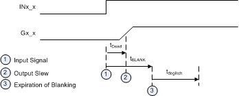 Figure 13. VDS Deglitch and Blank Diagram
The DRV8305 has three possible responses to a VDS overcurrent event. This response is set through the SPI VDS_MODE setting in register 0xC, bits D2-D0.
- VDS Latched Shutdown Mode:
- VDS Report Only Mode:
- VDS Disabled Mode:
When a VDS overcurrent event occurs, the device will pull all gate drive outputs low in order to put all six external MOSFETs into high impedance mode. The fault will be reported on the nFAULT pin with the specific MOSFET in which the overcurrent event was detected in reported through the SPI status registers.
In this mode, the device will take no action related to the gate drivers. When the overcurrent event is detected the fault will be reported on the nFAULT pin with the specific MOSFET in which the overcurrent event was detected in reported through the SPI status registers. The gate drivers will continue to operate normally.
The device ignores all the VDS overcurrent event detections and does not report them.
7.3.8.3.1 MOSFET dV/dt Turn On Protection (TDRIVE)
The DRV8305 gate driver implements a strong pulldown scheme during turn on of the opposite MOSFET for preventing parasitic dV/dt turn on. Parasitic dV/dt turn on can occur when charge couples into the gate of the low-side MOSFET during a switching event. If the charge induces enough voltage to cross the threshold of the low-side MOSFET shoot-through can occur in the half-bridge. To prevent this the TDRIVE: Gate Driver State Machine state machine turns on a strong pulldown during switching. After the switching event has completed, the gate driver switches back to a lower hold off pull down to improve efficiency.
7.3.8.3.2 MOSFET Gate Drive Protection (GDF)
The DRV8305 uses a multilevel scheme to protect the external MOSFET from VGS voltages that could damage it. The first stage uses integrated VGS clamps that will turn on when the GHx voltage exceeds the SHx voltage by a value that could be damaging to the external MOSFETs.
The second stage relies on the TDRIVE state machine to detect when abnormal conditions are present on the gate driver outputs. After the TDRIVE timer has expired the gate driver performs a check of the gate driver outputs against the commanded input. If the two do not match a gate drive fault (FETXX_VGS) is reported. This can be used to detected gate short to ground or gate short to supply event. The TDRIVE timer is adjustable for the high-side and low-side gate drive outputs through the TDRIVEN setting in register 0x5, bits D9-D8 and the TDRIVEP setting in register 0x6, bits D9-D8. The gate fault detection through TDRIVE can be disabled through the DIS_GDRV_FAULT setting in register 0x9, bit D8.
The third stage uses undervoltage monitors for the low-side gate drive regulator (VCP_LSD_UVLO2) and high-side gate drive charge pump (VCPH_UVLO2) and an overvoltage monitor for high-side charge pump (VCPH_OVLO). These monitors are used to detect if any of the power supplies to the gate drivers have encountered an abnormal condition.
7.3.8.4 Low-Side Source Monitors (SNS_OCP)
In additional to the VDS monitors across each MOSFET, the DRV8305 directly monitors the voltage on the SLx pins with respect to ground. If high current events such phase shorts cause the SLx pin voltage to exceed 2 V, the DRV8305 will shutdown the gate driver, put the external MOSFETs into a high impedance state, and report a SNS_OCP fault error on the nFAULT pin and corresponding SPI status bit in register 0x2, bits D2-D0.
7.3.8.5 Fault and Warning Operating Modes
Table 5. Fault and Warning Operating Modes(1)
| NAME | CONDITION | GATE DRIVE OUTPUTS | GATE DRIVE SUPPLIES | INTERNAL LOGIC | DEVICE ACTION |
|---|---|---|---|---|---|
| PVDD Undervoltage Fault (PVDD_UVLO) |
PVDD < VPVDD_UVLO1 | PL | D | D | - |
| PVDD < VPVDD_UVLO2 | PL | D | E | SPI nFAULT Latch |
|
| PVDD Undervoltage Warning (PVDD_UVFL) |
PVDD < VPVDD_UVFL | E | E | E | SPI nFAULT Toggle |
| PVDD Overvoltage Warning (PVDD_OVFL) |
PVDD > VPVDD_OVFL | E | E | E | SPI nFAULT Toggle |
| Charge Pump Undervoltage Warning (VCPH_UVFL) |
VCPH < VVCPH_UVFL | E | E | E | SPI nFAULT Toggle |
| Charge Pump Undervoltage Fault (VCPH_UVLO2) |
VCPH < VVCPH_UVLO2 | PL | D | E | SPI nFAULT Latch |
| LS Gate Supply Undervoltage Fault (VCP_LSD_UVLO2) |
VCP_LSD < VVCP_LSD_UVLO2 | PL | D | E | SPI nFAULT Latch |
| Charge Pump Overvoltage Fault (VCPH_OVLO) |
VCPH > VVCPH_OVLO | PL | D | E | SPI nFAULT Latch |
| VCPH > VVCPH_OVLO_ABS | PL | D | E | SPI nFAULT Latch |
|
| AVDD Undervoltage Fault (AVDD_UVLO) |
AVDD < VAVDD_UVLO | PL | D | E | SPI nFAULT Latch |
| Temperature Flag Warning (TEMP_FLAGX) |
TJ > TTEMP_FLAGX | E | E | E | SPI |
| Overtemperature Warning (OTW) |
TJ > TOTW | E | E | E | SPI nFAULT Toggle |
| Overtemperature Shutdown Fault (OTSD) |
TJ > TOTSD | PL | D | E | SPI nFAULT Latch |
| MOSFET Overcurrent Fault (VDS_OCP) |
Latched Shutdown VDS > VVDS_LEVEL |
PL | E | E | SPI nFAULT Latch |
| Report Only VDS > VVDS_LEVEL |
E | E | E | SPI nFAULT Toggle |
|
| Disabled VDS > VVDS_LEVEL |
E | E | E | - | |
| LS Overcurrent Fault (SNS_OCP) |
SLx > VSNS_OCP | PL | E | E | SPI nFAULT Latch |
| Gate Drive Fault (GDF) |
See TDRIVE | PL | D | E | SPI nFAULT Latch |
| MCU Watchdog Fault (WD_FAULT) |
tINTERVAL > tWD_DLY | PL | E | E | SPI PWRGD nFAULT Latch |
| VREG Undervoltage Fault (VREG_UV) |
VREG < VVREG_UV | PL | E | E | SPI PWRGD nFAULT Latch |
7.3.9 Undervoltage Warning (UVFL), Undervoltage Lockout (UVLO), and Overvoltage (OV) Protection
The DRV8305 implements undervoltage and overvoltage monitors on its system supplies to protect the system, prevent brownout conditons, and prevent unexpected device behavior. Undervoltage is monitored for on the PVDD, AVDD, VREF, VCPH, and VCP_LSD power supplies. Overvoltage is monitored for on the PVDD and VCPH power supplies. The values for the various undervoltage and overvoltage levels are provided in the electrical characteristics table under the voltage protection section.
The monitors for the main power supply, PVDD, incorporates several additional features:
- Undervoltage warning (PVDD_UVFL) level. Device operation is not impacted, report only indication.
- PVDD_UVFL is warning type error indicated on the nFAULT pin and the PVDD_UVFL status bit in register 0x1, bit D7
- Independent UVLO levels for the gate driver (PVDD_UVLO2) and VREG LDO regulator (PVDD_UVLO1). PVDD_UVLO2 will trigger a shutdown of the gate driver
- PVDD_UVLO2 is a fault type error indicated on the nFAULT pin and corresponding status bit in register 0x3, bit D10
- PVDD_UVLO2 may be disabled through the DIS_VPVDD_UVLO setting in register 0x9, bit D9. The fault will still be reported in the status bit in register 0x3, bit D10
- Overvoltage detection to monitor for load dump or supply pumping conditions. Device operation is not impacted, report only indication
- PVDD_OV is a warning type error indicated on the nFAULT pin and the PVDD_OV bit in register 0x1, bit D6
The monitors for the high-side charge pump supply, VCPH, and low-side supply (VCP_LSD) incorporate several additional features:
- VCPH relative (VCPH_OVLO) and absolute overvoltage (VCPH_OVLO_ABS) detection. The DRV8305 monitors VCPH for overvoltage conditions with respect to PVDD and GND
- VCPH_OVLO and VCPH_OVLO_ABS are fault type errors reported on nFAULT and the corresponding status bit in register 0x3, bits D1-D0
- VCPH undervoltage (VCPH_UVLO2) is monitored to prevent underdriven MOSFET conditions. VCPH_UVLO2 will trigger a shutdown of the gate driver
- VCPH_UVLO2 is a fault type error indicated on the nFAULT pin and corresponding status bit in register 0x3, bit D2
- VCP_LSD undervoltage (VCP_LSD_UVLO2) is monitored to prevent underdriven MOSFET conditions. VCP_LSD_UVLO2 will trigger a shutdown of the gate driver
- VCP_LSD_UVLO2 is a fault type error indicated on the nFAULT pin and corresponding status bit in register 0x3, bit D4
- Undervoltage proteciton for VCPH and VCP_LSD may not be disabled in the operating state
7.3.9.1 Overtemperature Warning (OTW) and Shutdown (OTSD) Protection
A multi-level temperature detection circuit is implemented in the DRV8305.
- Flag Level 1 (TEMP_FLAG1): Level 1 overtemperature flag. No warning reported on nFAULT. Real-time flag indicated in SPI register 0x1, bit D3.
- Flag Level 2 (TEMP_FLAG2): Level 2 overtemperature flag. No warning reported on nFAULT. Real-time flag indicated in SPI register 0x1, bit D2.
- Flag Level 3 (TEMP_FLAG3): Level 3 overtemperature flag. No warning reported on nFAULT. Real-time flag indicated in SPI register 0x1, bit D1.
- Flag Level 4 (TEMP_FLAG4): Level 4 overtemperature flag. No warning reported on nFAULT. Real-time flag indicated in SPI register 0x1, bit D8.
- Warning Level (OTW): Overtemperature warning only. Warning reported on nFAULT. Real-time flag indicated in SPI register 0x1, bit D0.
- Fault Level (OTSD): Overtemperature fault and latched shut down of the device. Fault reported on nFAULT and in SPI register 0x3, bit D8.
SPI operation is still available and register settings will be retained in the device during OTSD operation as long as PVDD is within operation range. An OTSD fault can be cleared when the device temperature has dropped below the fault level and a CLR_FLTS is issued.
7.3.9.2 Reverse Supply Protection
The DRV8305 is designed to support an external reverse supply protection scheme. The VCPH high-side charge pump is able to supply an external load up to 10 mA. This feature allows implementation of an external reverse battery protection scheme using a MOSFET and a BJT. The MOSFET gate and BJT can be driven through VCPH with a current limiting resistor. The current limiting resistor must be sized not to exceed the maximum external load on VCPH.
The VDRAIN sense pin may also be protected against reverse supply conditions by use of a current limiting resistor. The current limit resistor must be sized not to exceed the maximum current load on the VDRAIN pin. 100 Ω is recommended between VDRAIN and the drain of the external high-side MOSFET.
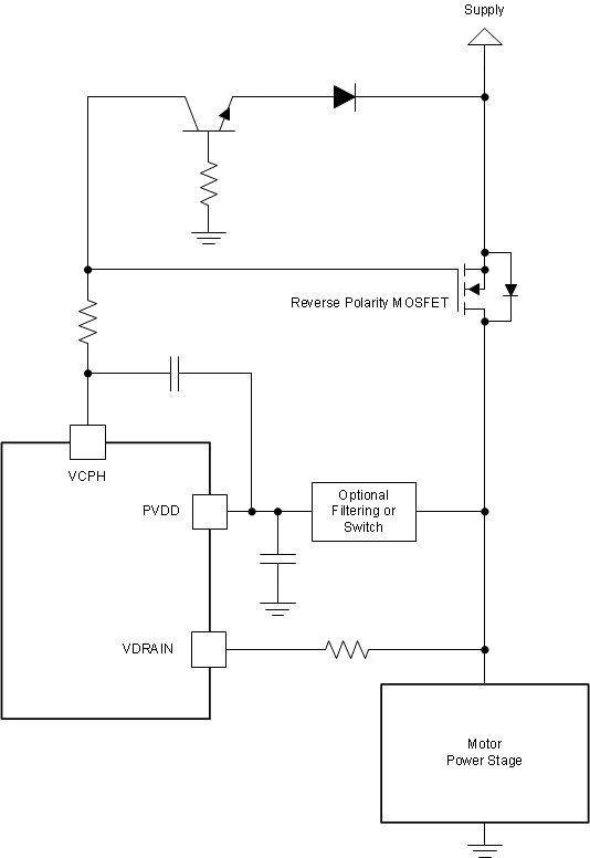 Figure 14. Typical Scheme for Reverse Battery Protection Using VCPH
7.3.9.3 MCU Watchdog
The DRV8305 incorporates an MCU watchdog function to ensure that the external controller that is instructing the device is active and not in an unknown state. The MCU watchdog function may be enabled by writing a 1 to the WD_EN setting in the SPI register 0x9. bit D3. The default setting for the device is with the watchdog disabled. When the watchdog is enabled, an internal timer starts to countdown to the interval set by the WD_DLY setting in the SPI register 0x9, bits D6-D5. To restart the watchdog timer, the address 0x1 (status register) must be read by the controller within the interval set by the WD_DLY setting. If the watchdog timer is allowed to expire without the address 0x1 being read, a watchdog fault will be enabled.
Response to a watchdog fault is as follows:
- A latched fault occurs on the DRV8305 and the gate drivers are put into a safe state. An appropriate recovery sequence must then be performed.
- The PWRGD pin is taken low for 56 µs and then back high in order to reset the controller or indicate the watchdog fault
- The nFAULT pin is asserted low, the WD_EN bit is cleared, and the WD_FAULT set high in register 0x3, bit D9
- It is recommended to read the status registers as part of the recovery or power-up routine in order to determine whether a WD_FAULT had previously occurred
Note that the watchdog fault results in a clearing of the WD_EN setting and it will have to be set again to resume watchdog functionality.
7.3.9.4 VREG Undervoltage (VREG_UV)
The DRV8305 has an undervoltage monitor on the VREG output regulator to ensure the external controller does not experience a brownout condition. The undervoltage monitor will signal a fault if the VREG output drops below a set threshold from its set point. The VREG output set point is configured for two different levels, 3.3 V or 5 V, depending on the DRV8305 device options (DRV83053Q and DRV83055Q). The VREG undervoltage level can be set through the SPI setting VREG_UV_LEVEL in register 0xB, bits D1-D0. The VREG undervoltage monitor can be disabled through the SPI setting DIS_VREG_PWRGD in register 0xB, bit D2.
Response to a VREG undervoltage fault is as follows:
- A latched fault occurs on the DRV8305 and the gate drivers are put into a safe state. An appropriate recovery sequence must then be performed.
- The PWRGD is taken low until the undervoltage condition is removed and for at least a minimum of 56 µs.
- The nFAULT pin is asserted low and the VREG_UV bit set high in register 0x3, bit D6.
- The fault can be cleared after the VREG undervoltage condition is removed with CLR_FLTS or an EN_GATE reset pulse
Note that the VREG undervoltage monitor is disabled on the no regulator (VREF) device option (DRV8305NQ and DRV8305NE).
7.4 Device Functional Modes
7.4.1 Power Up Sequence
The DRV8305 has an internal state machine to ensure proper power up and power down sequencing of the device. When PVDD power is applied the device will remain inactive until PVDD cross the digital logic threshold. At this point, the digital logic will become active, VREG will enable (if 3.3V or 5V device option is used), the passive gate pull downs will enable, and nFAULT will be driven low to indicate that the device has not reached the VPVDD_UVLO2 threshold. nFAULT will remain driven low until PVDD crosses the PVDD_UVLO threshold. At this point the device will enter its standby state.
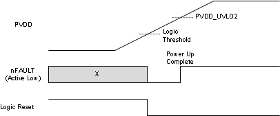 Figure 15. Power-Up Sequence
7.4.2 Standby State
After the power up sequence is completed and the PVDD voltage is above VPVDD_UVLO2 threshold, the DRV8305 will indicate successful and fault free power up of all circuits by releasing the nFAULT pin. At this point the DRV8305 will enter its standby state and be ready to accept inputs from the external controller. The DRV8305 will remain in or re-enter its standby state anytime EN_GATE = LOW or a fault type error has occured. In this state the major gate driver blocks are disabled, but the passive gate pulldowns are still active to maintain the external MOSFETs in their high impedence state. It is recommended, but not required to perform all device configurations through SPI in the standby state.
7.4.3 Operating State
After reaching the standby state and then taking EN_GATE from LOW to HIGH, the DRV8305 will enter its operating state. The operating state enables the major gate driver and current shunt amplifier blocks for normal operation. 1 ms should be allowed after EN_GATE is taken HIGH to allow the charge pump supply for the high-side gate drivers to reach its steady state operating point. If at any point in its operating state a fault type error occurs, the DRV8305 will immedietely re-enter the standby state.
7.4.4 Sleep State
The sleep state can be entered by issuing a sleep command through the SLEEP bit in SPI register 0x9, bit D2 with the device in its standby state (EN_GATE = LOW). The device will not respond to a sleep command in its operating state. After the sleep command is received, the gate drivers and output regulator (VREG) will safely power down after a programmable delay set in the SPI register 0xB, bits D4-D3. The device can then only be enabled through the WAKE pin which is a high-voltage tolerant input pin. For the DRV8305 to be brough out of sleep, the WAKE pin must be at a voltage greater than 3 V. This allows the wake pin to be driven, for example, directly by the battery through a switch, through the inhibit pin (INH) on a standard LIN interface, or through standard digital logic. The WAKE pin will only react to a wake up command if PVDD > VPVDD_UVLO2. After the DRV8305 is out of SLEEP mode, all activity on the WAKE pin is ignored. The sleep state erases all values in the SPI control registers and it is not recommended to write through SPI in the sleep state.
7.4.5 Limp Home or Fail Code Operation
The DRV8305 enables the adoption of secondary limp-home or fail code software through configurable fault mode handling. The following device features may be configured during the operating state without stopping the motor.
- IDRIVE Gate Current Output (IDRIVEN_HS, IDRIVEP_HS, IDRIVEN_LS, IDRIVEP_LS): All four IDRIVEX settings may be adjusted during normal operation without issue. This features allows the software to change the slew rate, switching characteristics of the external MOSFETs on the fly if required without having to stop the motor rotation. The IDRIVEX settings are located in the SPI registers 0x5 (high-side) and 0x6 (low-side)
- VDS Fault Mode (VDS_MODE): The VDS overcurrent monitors may be changed from latched shut down (VDS_MODE = b'000) or report only (VDS_MODE = b'001) modes to disabled (VDS_MODE = b'010) mode to allow operation of the external MOSFETs past normal operating conditions. This is the only VDS_MODE change allowed in the operating state. The VDS_MODE setting is located in the SPI register 0xC, bits D2-D0.
- VDS Comparator Thresholds (VDS_LEVEL): The VDS overcurrent monitor threshold (VDS_LEVEL) may be changed at any time during operation to allow for higher that standard operating currents. The VDS_LEVEL setting is located in the SPI register 0xC.
- VGS Fault Mode (DIS_GDRV_FAULT): The VGS fault detection monitors can be disabled through the SPI register 0x9, bit D8. Reporting in SPI will also be disabled as a result.
- SNS_OCP Fault Mode (DIS_SNS_OCP): The sense amplifer overcurrent monitors can be disabled through the SPI register 0x9, bit D4. Reporting in SPI will also be disabled as a result.
- PVDD Underoltage Lockout (DIS_VPVDD_UVLO2): The main power supply undervoltage lockout can be disabled through the SPI register 0x9, but D9. Reporting in SPI will also be disabled as a result.
- OTSD Overtemperature Shutdown (FLIP_OTS): The overtemperature shutdown can be disabled through the SPI register 0x9, bit D10. Reporting in SPI will also be disabled as a result. The OTS overtemperature shutdown is disabled by default on the Grade 0, DRV8305xE device.
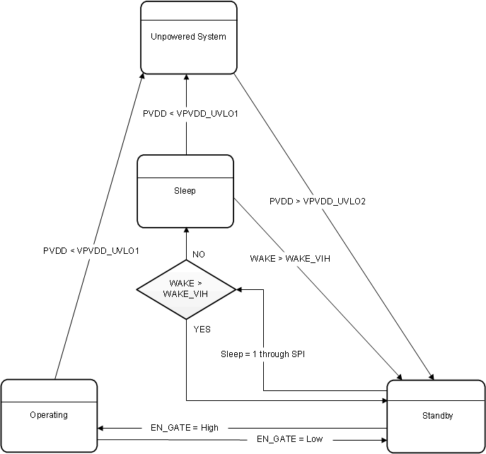 Figure 16. Operating States
7.5 Programming
7.5.1 SPI Communication
7.5.1.1 SPI
The DRV8305 uses a SPI to set device configurations, operating parameters, and read out diagnostic information. The DRV8305 SPI operates in slave mode. The SPI input data (SDI) word consists of a 16 bit word with a 5 bit command and 11 bits of data. The SPI output data (SDO) word consists of 11 bits of register data with the first 5 bits (MSB) as don't cares.
A valid frame must meet following conditions:
- CPOL (clock polarity) = 0 and CPHA (clock phase) = 1
- SCLK must be low when nSCS transistions
- Full 16 SCLK cycles
- Data is always propogated on the rising edge of SCLK
- Data is always captured on the falling edge of SCLK
- MSB is shifted in and out first
- When nSCS is high, SCLK and SDI are ignored and SDO is high impedance
- nSCS should be taken high for at least 500 ns between frames
- If the data sent to SDI is less than or greater than 16 bits it is considered a frame error and the data will be ignored.
7.5.1.2 SPI Format
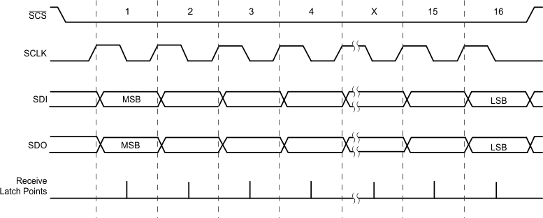 Figure 17. SPI Slave Mode Timing Diagram
The SPI input data (SDI) control word is 16 bits long and consists of the following format:
- 1 read or write bit W [15]
- 4 address bits A [14:11]
- 11 data bits D [10:0]
The SPI output data (SDO) word response word is 11 bits long (first 5 bits are don't cares). It contains the content of the register being accessed.
The MSB of the SDI word (W0) is the read/write bit. When W0 = 0, the input data is a write command. When W0 = 1, the input data is a read command.
For a write command: The response word is the data currently in the register being written to.
For a read command: The response word is the data currently in the register being read.
Table 6. SPI Input Data Control Word Format
| R/W | ADDRESS | DATA | ||||||||||||||
|---|---|---|---|---|---|---|---|---|---|---|---|---|---|---|---|---|
| Word Bit | B15 | B14 | B13 | B12 | B11 | B10 | B9 | B8 | B7 | B6 | B5 | B4 | B3 | B2 | B1 | B0 |
| Command | W0 | A3 | A2 | A1 | A0 | D10 | D9 | D8 | D7 | D6 | D5 | D4 | D3 | D2 | D1 | D0 |
Table 7. SPI Output Data Response Word Format
| DATA | ||||||||||||||||
|---|---|---|---|---|---|---|---|---|---|---|---|---|---|---|---|---|
| Word Bit | B15 | B14 | B13 | B12 | B11 | B10 | B9 | B8 | B7 | B6 | B5 | B4 | B3 | B2 | B1 | B0 |
| Command | X | X | X | X | X | D10 | D9 | D8 | D7 | D6 | D5 | D4 | D3 | D2 | D1 | D0 |
7.6 Register Maps
Table 8. Register Map
| ADDRESS | NAME | D10 | D9 | D8 | D7 | D6 | D5 | D4 | D3 | D2 | D1 | D0 |
|---|---|---|---|---|---|---|---|---|---|---|---|---|
| 0x1 | Warnings & Watchdog Reset | FAULT | RSVD | TEMP_FLAG4 | PVDD_UVFL | PVDD_OVFL | VDS_STATUS | VCPH_UVFL | TEMP_FLAG1 | TEMP_FLAG2 | TEMP_FLAG3 | OTW |
| 0x2 | OV/VDS Faults |
VDS_HA | VDS_LA | VDS_HB | VDS_LB | VDS_HC | VDS_LC | RSVD | SNS_C_OCP | SNS_B_OCP | SNS_A_OCP | |
| 0x3 | IC Faults |
PVDD_UVLO2 | WD_FAULT | OTSD | RSVD | VREG_UV | AVDD_UVLO | VCP_LSD _UVLO2 |
RSVD | VCPH_UVLO2 | VCPH_OVLO | VCPH_OVLO _ABS |
| 0x4 | VGS Faults |
VGS_HA | VGS_LA | VGS_HB | VGS_LB | VGS_HC | VGS_LC | RSVD | ||||
| 0x5 | HS Gate Drive Control | RSVD | TDRIVEN | IDRIVEN_HS | IDRIVEP_HS | |||||||
| 0x6 | LS Gate Drive Control | RSVD | TDRIVEP | IDRIVEN_LS | IDRIVEP_LS | |||||||
| 0x7 | Gate Drive Control | RSVD | COMM_OPTION | PWM_MODE | DEAD_TIME | TBLANK | TVDS | |||||
| 0x8 | Reserved | RSVD | ||||||||||
| 0x9 | IC Operation | FLIP_OTSD | DIS_PVDD _UVLO2 |
DIS_GDRV _FAULT |
EN_SNS _CLAMP |
WD_DLY | DIS_SNS_OCP | WD_EN | SLEEP | CLR_FLTS | SET_VCPH_UV | |
| 0xA | Shunt Amplifier Control | DC_CAL_CH3 | DC_CAL_CH2 | DC_CAL_CH1 | CS_BLANK | GAIN_CS3 | GAIN_CS2 | GAIN_CS1 | ||||
| 0xB | Voltage Regulator Control | RSVD | VREF_SCALE | RSVD | SLEEP_DLY | DIS_VREG _PWRGD |
VREG_UV_LEVEL | |||||
| 0xC | VDS Sense Control | RSVD | VDS_LEVEL | VDS_MODE | ||||||||
7.6.1 Status Registers
The status registers are used to report device warnings, fault conditions, and provide a means to prevent timing out of the watchdog timer. Status registers are read only registers.
7.6.1.1 Warning and Watchdog Reset (Address = 0x1)
Table 9. Warning and Watchdog Reset Register Description
| BIT | R/W | NAME | DEFAULT | DESCRIPTION |
|---|---|---|---|---|
| 10 | R | FAULT | 0x0 | Fault indication |
| 9 | R | RSVD | 0x0 | - |
| 8 | R | TEMP_FLAG4 | 0x0 | Temperature flag setting for approximately 175°C |
| 7 | R | PVDD_UVFL | 0x0 | PVDD undervoltage flag warning |
| 6 | R | PVDD_OVFL | 0x0 | PVDD overvoltage flag warning |
| 5 | R | VDS_STATUS | 0x0 | Real time OR of all VDS overcurrent monitors |
| 4 | R | VCHP_UVFL | 0x0 | Charge pump undervoltage flag warning |
| 3 | R | TEMP_FLAG1 | 0x0 | Temperature flag setting for approximately 105°C |
| 2 | R | TEMP_FLAG2 | 0x0 | Temperature flag setting for approximately 125°C |
| 1 | R | TEMP_FLAG3 | 0x0 | Temperature flag setting for approximately 135°C |
| 0 | R | OTW | 0x0 | Overtemperature warning |
7.6.1.2 OV/VDS Faults (Address = 0x2)
Table 10. OV/VDS Faults Register Description
| BIT | R/W | NAME | DEFAULT | DESCRIPTION |
|---|---|---|---|---|
| 10 | R | VDS_HA | 0x0 | VDS overcurrent fault for high-side MOSFET A |
| 9 | R | VDS_LA | 0x0 | VDS overcurrent fault for low-side MOSFET A |
| 8 | R | VDS_HB | 0x0 | VDS overcurrent fault for high-side MOSFET B |
| 7 | R | VDS_LB | 0x0 | VDS overcurrent fault for low-side MOSFET B |
| 6 | R | VDS_HC | 0x0 | VDS overcurrent fault for high-side MOSFET C |
| 5 | R | VDS_LC | 0x0 | VDS overcurrent fault for low-side MOSFET C |
| 4:3 | R | RSVD | 0x0 | - |
| 2 | R | SNS_C_OCP | 0x0 | Sense C overcurrent fault |
| 1 | R | SNS_B_OCP | 0x0 | Sense B overcurrent fault |
| 0 | R | SNS_A_OCP | 0x0 | Sense A overcurrent fault |
7.6.1.3 IC Faults (Address = 0x3)
Table 11. IC Faults Register Description
| BIT | R/W | NAME | DEFAULT | DESCRIPTION |
|---|---|---|---|---|
| 10 | R | PVDD_UVLO2 | 0x0 | PVDD undervoltage 2 fault |
| 9 | R | WD_FAULT | 0x0 | Watchdog fault |
| 8 | R | OTSD | 0x0 | Overtemperature fault |
| 7 | R | RSVD | 0x0 | - |
| 6 | R | VREG_UV | 0x0 | VREG undervoltage fault |
| 5 | R | AVDD_UVLO | 0x0 | AVDD undervoltage fault |
| 4 | R | VCP_LSD_UVLO2 | 0x0 | Low-side gate supply fault |
| 3 | R | RSVD | 0x0 | - |
| 2 | R | VCPH_UVLO2 | 0x0 | High-side charge pump undervoltage 2 fault |
| 1 | R | VCPH_OVLO | 0x0 | High-side charge pump overvoltage fault |
| 0 | R | VCPH_OVLO_ABS | 0x0 | High-side charge pump overvoltage ABS fault |
7.6.1.4 VGS Faults (Address = 0x4)
Table 12. Gate Driver VGS Faults Register Description
| BIT | R/W | NAME | DEFAULT | DESCRIPTION |
|---|---|---|---|---|
| 10 | R | VGS_HA | 0x0 | VGS gate drive fault for high-side MOSFET A |
| 9 | R | VGS_LA | 0x0 | VGS gate drive fault for low-side MOSFET A |
| 8 | R | VGS_HB | 0x0 | VGS gate drive fault for high-side MOSFET B |
| 7 | R | VGS_LB | 0x0 | VGS gate drive fault for low-side MOSFET B |
| 6 | R | VGS_HC | 0x0 | VGS gate drive fault for high-side MOSFET C |
| 5 | R | VGS_LC | 0x0 | VGS gate drive fault for low-side MOSFET C |
| 4:0 | R | RSVD | 0x0 | - |
7.6.2 Control Registers
Control registers are used to set the device parameters for DRV8305-Q1. The default values are shown in bold.
- Control registers are read/write registers
- Do not clear on register read, CLR_FLTs, or EN_GATE resets
- Cleared to default values on power up
- Cleared to default values when the device enters SLEEP mode
7.6.2.1 HS Gate Drive Control (Address = 0x5)
Table 13. HS Gate Driver Control Register Description
| BIT | R/W | NAME | DEFAULT | DESCRIPTION | |||
|---|---|---|---|---|---|---|---|
| 10 | R/W | RSVD | 0x0 | - | |||
| 9:8 | R/W | TDRIVEN | 0x3 | High-side gate driver peak source time b'00 - 220 ns b'01 - 440 ns b'10 - 880 ns b'11 - 1780 ns |
|||
| 7:4 | R/W | IDRIVEN_HS | 0x4 | High-side gate driver peak sink current | |||
| b'0000 - 20 mA b'0100 - 60 mA b'1000 - 0.50 A b'1100 - 60 mA |
b'0001 - 30 mA b'0101 - 70 mA b'1001 - 0.75 A b'1101 - 60 mA |
b'0010 - 40 mA b'0110 - 80 mA b'1010 - 1.00 A b'1110 - 60 mA |
b'0011 - 50 mA b'0111 - 0.25 A b'1011 - 1.25 A b'1111 - 60 mA |
||||
| 3:0 | R/W | IDRIVEP_HS | 0x4 | High-side gate driver peak source current | |||
| b'0000 - 10 mA b'0100 - 50 mA b'1000 - 0.25 A b'1100 - 50 mA |
b'0001 - 20 mA b'0101 - 60 mA b'1001 - 0.50 A b'1101 - 50 mA |
b'0010 - 30 mA b'0110 - 70 mA b'1010 - 0.75 A b'1110 - 50 mA |
b'0011 - 40 mA b'0111 - 0.125 A b'1011 - 1.00 A b'1111 - 50 mA |
||||
7.6.2.2 LS Gate Drive Control (Address = 0x6)
Table 14. LS Gate Driver Control Register Description
| BIT | R/W | NAME | DEFAULT | DESCRIPTION | |||
|---|---|---|---|---|---|---|---|
| 10 | R/W | RSVD | 0x0 | - | |||
| 9:8 | R/W | TDRIVEP | 0x3 | Low-side gate driver peak source time b'00 - 220 ns b'01 - 440 ns b'10 - 880 ns b'11 - 1780 ns |
|||
| 7:4 | R/W | IDRIVEN_LS | 0x4 | Low-side gate driver peak sink current | |||
| b'0000 - 20 mA b'0100 - 60 mA b'1000 - 0.50 A b'1100 - 60 mA |
b'0001 - 30 mA b'0101 - 70 mA b'1001 - 0.75 A b'1101 - 60 mA |
b'0010 - 40 mA b'0110 - 80 mA b'1010 - 1.00 A b'1110 - 60 mA |
b'0011 - 50 mA b'0111 - 0.25 A b'1011 - 1.25 A b'1111 - 60 mA |
||||
| 3:0 | R/W | IDRIVEP_LS | 0x4 | Low-side gate driver peak source current | |||
| b'0000 - 10 mA b'0100 - 50 mA b'1000 - 0.25 A b'1100 - 50 mA |
b'0001 - 20 mA b'0101 - 60 mA b'1001 - 0.50 A b'1101 - 50 mA |
b'0010 - 30 mA b'0110 - 70 mA b'1010 - 0.75 A b'1110 - 50 mA |
b'0011 - 40 mA b'0111 - 0.125 A b'1011 - 1.00 A b'1111 - 50 mA |
||||
7.6.2.3 Gate Drive Control (Address = 0x7)
Table 15. Gate Drive Control Register Description
| BIT | R/W | NAME | DEFAULT | DESCRIPTION | ||
|---|---|---|---|---|---|---|
| 10 | R/W | RSVD | 0x0 | - | ||
| 9 | R/W | COMM_OPTION | 0x1 | Rectification control (PWM_MODE = b'10 only) b'0 - diode freewheeling b'1 - active freewheeling |
||
| 8:7 | R/W | PWM_MODE | 0x0 | PWM Mode b'00 - PWM with 6 independent inputs b'01 - PWM with 3 independent inputs b'10 - PWM with one input b'11 - PWM with 6 independent inputs |
||
| 6:4 | R/W | DEAD_TIME | 0x1 | Dead time | ||
| b'000 - 35 ns b'011 - 440 ns b'110 - 3520 ns |
b'001 - 52 ns
b'100 - 880 ns b'111 - 5280 ns |
b'010 - 88 ns b'101 - 1760 ns |
||||
| 3:2 | R/W | TBLANK | 0x1 | VDS sense blanking b'00 - 0 µs b'01 - 1.75 µs b'10 - 3.5 µs b'11 - 7 µs |
||
| 1:0 | R/W | TVDS | 0x2 | VDS sense deglitch b'00 - 0 µs b'01 - 1.75 µs b'10 - 3.5 µs b'11 - 7 µs |
||
7.6.2.4 IC Operation (Address = 0x9)
Table 16. IC Operation Register Description
| BIT | R/W | NAME | DEFAULT | DESCRIPTION |
|---|---|---|---|---|
| 10 | R/W | FLIP_OTSD | 0x0 | Enable OTSD b'0 - Disable OTSD b'1 - Enable OTSD |
| 9 | R/W | DIS_PVDD_UVLO2 | 0x0 | Disable PVDD_UVLO2 fault and reporting b'0 - PVDD_UVLO2 enabled b'1 - PVDD_UVLO2 disabled |
| 8 | R/W | DIS_GDRV_FAULT | 0x0 | Disable gate drive fault and reporting b'0 - Gate driver fault enabled b'1 - Gate driver fault disabled |
| 7 | R/W | EN_SNS_CLAMP | 0x0 | Enable sense amplifier clamp b'0 - Sense amplifier clamp is not enabled b'1 - Sense amplifier clamp is enabled, limiting output to ~3.3 V |
| 6:5 | R/W | WD_DLY | 0x1 | Watchdog delay b'00 - 10 ms b'01 - 20 ms b'10 - 50 ms b'11 - 100 ms |
| 4 | R/W | DIS_SNS_OCP | 0x0 | Disable SNS overcurrent protection fault and reporting b'0 - SNS OCP enabled b'1 - SNS OCP disabled |
| 3 | R/W | WD_EN | 0x0 | Watchdog enable b'0 - Watch dog disabled b'1 - Watch dog enabled |
| 2 | R/W | SLEEP | 0x0 | Put device into sleep mode b'0 - Device awake b'1 - Device asleep |
| 1 | R/W | CLR_FLTS | 0x0 | Clear faults b'0 - Normal operation b'1 - Clear faults |
| 0 | R/W | SET_VCPH_UV | 0x0 | Set charge pump undervoltage threshold level b'0 - 4.9 V b'1 - 4.6 V |
7.6.2.5 Shunt Amplifier Control (Address = 0xA)
Table 17. Shunt Amplifier Control Register Description
| BIT | R/W | NAME | DEFAULT | DESCRIPTION |
|---|---|---|---|---|
| 10 | R/W | DC_CAL_CH3 | 0x0 | DC calibration of CS amplifier 3 b'0 - Normal operation b'1 - DC calibration mode |
| 9 | R/W | DC_CAL_CH2 | 0x0 | DC calibration of CS amplifier 2 b'0 - Normal operation b'1 - DC calibration mode |
| 8 | R/W | DC_CAL_CH1 | 0x0 | DC calibration of CS amplifier 1 b'0 - Normal operation b'1 - DC calibration mode |
| 7:6 | R/W | CS_BLANK | 0x0 | Current shunt amplifier blanking time b'00 - 0 ns b'01 - 500 ns b'10 - 2.5 µs b'11 - 10 µs |
| 5:4 | R/W | GAIN_CS3 | 0x0 | Gain of CS amplifier 3 b'00 - 10 V/V b'01 - 20 V/V b'10 - 40 V/V b'11 - 80 V/V |
| 3:2 | R/W | GAIN_CS2 | 0x0 | Gain of CS amplifier 2 b'00 - 10 V/V b'01 - 20 V/V b'10 - 40 V/V b'11 - 80 V/V |
| 1:0 | R/W | GAIN_CS1 | 0x0 | Gain of CS amplifier 1 b'00 - 10 V/V b'01 - 20 V/V b'10 - 40 V/V b'11 - 80 V/V |
7.6.2.6 Voltage Regulator Control (Address = 0xB)
Table 18. Voltage Regulator Control Register Description
| BIT | R/W | NAME | DEFAULT | DESCRIPTION |
|---|---|---|---|---|
| 10 | R/W | RSVD | 0x0 | - |
| 9:8 | R/W | VREF_SCALE | 0x1 | VREF Scaling b'00 - RSVD b'01 - k = 2 b'10 - k = 4 b'11 - RSVD |
| 7:5 | R/W | RSVD | 0x0 | - |
| 4:3 | R/W | SLEEP_DLY | 0x1 | Delay to power down VREG after SLEEP b'00 - 0 µs b'01 - 10 µs b'10 - 50 µs b'11 - 1 ms |
| 2 | R/W | DIS_VREG_PWRGD | 0x0 | Disable VREG undervoltage fault and reporting b'0 - VREG_UV enabled b'1 - VREG_UV disabled |
| 0:1 | R/W | VREG_UV_LEVEL | 0x2 | VREG undervoltage set point b'00 - VREG x 0.9 b'01 - VREG x 0.8 b'10 - VREG x 0.7 b'11 - VREG x 0.7 |
7.6.2.7 VDS Sense Control (Address = 0xC)
Table 19. VDS Sense Control Register Description
| BIT | R/W | NAME | DEFAULT | DESCRIPTION | |||
|---|---|---|---|---|---|---|---|
| 10:8 | R/W | RSVD | 0x0 | - | |||
| 7:3 | R/W | VDS_LEVEL | 0x19 | VDS comparator threshold | |||
| b'00000 - 0.060 V b'00100 - 0.097 V b'01000 - 0.155 V b'01100 - 0.250 V b'10000 - 0.403 V b'10100 - 0.648 V b'11000 - 1.043 V b'11100 - 1.679 V |
b'00001 - 0.068 V b'00101 - 0.109 V b'01001 - 0.175 V b'01101 - 0.282 V b'10001 - 0.454 V b'10101 - 0.730 V b'11001 - 1.175 V b'11101 - 1.892 V |
b'00010 - 0.076 V b'00110 - 0.123 V b'01010 - 0.197V b'01110 - 0.317 V b'10010 - 0.511 V b'10110 - 0.822 V b'11010 - 1.324 V b'11110 - 2.131 V |
b'00011 - 0.086 V b'00111 - 0.138 V b'01011 - 0.222 V b'01111 - 0.358 V b'10011 - 0.576 V b'10111 - 0.926 V b'11011 - 1.491 V b'11111 - 2.131 V |
||||
| 2:0 | R/W | VDS_MODE | 0x0 | VDS mode b'000 - Latched shut down when over-current detected b'001 - Report only when over current detected b'010 - VDS protection disabled (no overcurrent sensing or reporting) |
|||