SLVSCK2A April   2014  – February 2016 DRV8307

PRODUCTION DATA.  

  1. Features
  2. Applications
  3. Description
  4. Revision History
  5. Pin Configurations and Functions
  6. Specifications
    1. 6.1 Absolute Maximum Ratings
    2. 6.2 ESD Ratings
    3. 6.3 Recommended Operating Conditions
    4. 6.4 Thermal Information
    5. 6.5 Electrical Characteristics
    6. 6.6 Timing Requirements
    7. 6.7 Typical Characteristics
  7. Detailed Description
    1. 7.1 Overview
    2. 7.2 Functional Block Diagram
    3. 7.3 Feature Description
      1. 7.3.1  Hall Comparators
      2. 7.3.2  HALLOUT Output
      3. 7.3.3  Enable, Reset, and Clock Generation
      4. 7.3.4  Commutation
        1. 7.3.4.1 120° 3-Hall Commutation
        2. 7.3.4.2 120° Single-Hall Commutation
      5. 7.3.5  Braking
      6. 7.3.6  Output Pre-Drivers
      7. 7.3.7  Current Limit
      8. 7.3.8  Charge Pump
      9. 7.3.9  5-V Linear Regulator
      10. 7.3.10 Power Switch
      11. 7.3.11 Protection Circuits
        1. 7.3.11.1 VM Undervoltage Lockout (UVLO)
        2. 7.3.11.2 VM Overvoltage (VMOV)
        3. 7.3.11.3 Motor Overcurrent Protection (OCP)
        4. 7.3.11.4 Charge Pump Failure (CPFAIL)
        5. 7.3.11.5 Charge Pump Short (CPSC)
        6. 7.3.11.6 Rotor Lockup (RLOCK)
        7. 7.3.11.7 Overtemperature (OTS)
    4. 7.4 Device Functional Modes
      1. 7.4.1 Clock PWM Mode
  8. Application and Implementation
    1. 8.1 Application Information
      1. 8.1.1 Hall Sensor Configurations and Connections
      2. 8.1.2 ENABLEn Considerations
      3. 8.1.3 Faster Starting and Stopping
    2. 8.2 Typical Application
      1. 8.2.1 Design Requirements
      2. 8.2.2 Detailed Design Procedure
      3. 8.2.3 Application Performance Plot
  9. Power Supply Recommendations
  10. 10Layout
    1. 10.1 Layout Guidelines
    2. 10.2 Layout Example
  11. 11Device and Documentation Support
    1. 11.1 Trademarks
    2. 11.2 Electrostatic Discharge Caution
    3. 11.3 Glossary
  12. 12Mechanical, Packaging, and Orderable Information

Package Options

Mechanical Data (Package|Pins)
Thermal pad, mechanical data (Package|Pins)
Orderable Information

10 Layout

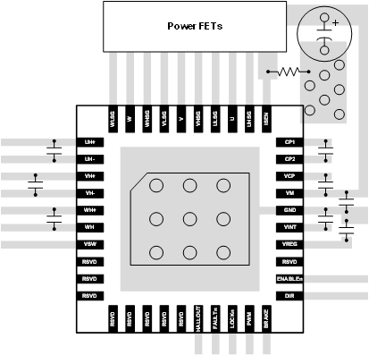
10.1 Layout Guidelines

For VM, place 0.1-μF bypass capacitor close to the device. Take care to minimize the loop formed by the bypass capacitor connection from VM to GND.

10.2 Layout Example

DRV8307 8307lay.gif