SLVSCK2A April 2014 – February 2016 DRV8307
PRODUCTION DATA.
- 1 Features
- 2 Applications
- 3 Description
- 4 Revision History
- 5 Pin Configurations and Functions
- 6 Specifications
-
7 Detailed Description
- 7.1 Overview
- 7.2 Functional Block Diagram
- 7.3 Feature Description
- 7.4 Device Functional Modes
- 8 Application and Implementation
- 9 Power Supply Recommendations
- 10Layout
- 11Device and Documentation Support
- 12Mechanical, Packaging, and Orderable Information
Package Options
Mechanical Data (Package|Pins)
- RHA|40
Thermal pad, mechanical data (Package|Pins)
- RHA|40
Orderable Information
6 Specifications
6.1 Absolute Maximum Ratings
over operating free-air temperature (unless otherwise noted) (1)(2)(3)| MIN | MAX | UNIT | |
|---|---|---|---|
| Power supply voltage (VM) | –0.3 | 42 | V |
| Charge pump and high-side gate drivers (VCP, UHSG, VHSG, WHSG) | –0.3 | 50 | V |
| Output terminal, low side gate drivers, charge pump flying cap and switched VM power supply voltage (U, V, W, ULSG, VLSG, WLSG, CP1, CP2 VSW) | –0.6 | 40 | V |
| Internal core voltage regulator (VINT) | –0.3 | 2.0 | V |
| Linear voltage regulator output (VREG) | –0.3 | 5.5 | V |
| Sense current terminal (ISEN) | –0.3 | 2.0 | V |
| Digital terminal voltage (FAULTn, LOCKn, PWM, BRAKE, DIR, ENABLEn, HALLOUT) | –0.5 | 5.75 | V |
| Hall sensor input terminal voltage (HU+, HU–, HV+, HV–, HW+, HW–) | 0 | VREG | V |
| Continuous total power dissipation | See Thermal Information | ||
| Operating junction temperature range, TJ | –40 | 150 | °C |
| Storage temperature range, Tstg | –60 | 150 | °C |
(1) Stresses beyond those listed under “absolute maximum ratings” may cause permanent damage to the device. These are stress ratings only, and functional operation of the device at these or any other conditions beyond those indicated under “recommended operating conditions” is not implied. Exposure to absolute–maximum–rated conditions for extended periods may affect device reliability.
(2) All voltage values are with respect to network ground terminal.
(3) Power dissipation and thermal limits must be observed
6.2 ESD Ratings
| VALUE | UNIT | |||
|---|---|---|---|---|
| V(ESD) | Electrostatic discharge | Human-body model (HBM), per ANSI/ESDA/JEDEC JS-001(1) | ±4000 | V |
| Charged-device model (CDM), per JEDEC specification JESD22-C101(2) | ±1500 | |||
(1) JEDEC document JEP155 states that 500-V HBM allows safe manufacturing with a standard ESD control process.
(2) JEDEC document JEP157 states that 250-V CDM allows safe manufacturing with a standard ESD control process.
6.3 Recommended Operating Conditions
over operating free-air temperature range (unless otherwise noted)| MIN | NOM | MAX | UNIT | |||
|---|---|---|---|---|---|---|
| VM | Motor power supply voltage range, ENABLEn = 0, motor operating (3) | 8.5 | 32 | V | ||
| VMDIS | Motor power supply voltage range, ENABLEn = 1, motor not operating | 4.5 | 35 | |||
| IVREG | VREG output current(1) | 0 | 30 | mA | ||
| IVSW | VSW output current(1) | 0 | 30 | |||
| fHALL | Hall sensor input frequency(4) | 0 | 30 | kHz | ||
| fPWM | Frequency on PWM | 16 | 50 (2) | kHz | ||
(1) Power dissipation and thermal limits must be observed
(2) Operational with frequencies above 50 kHz, but resolution is degraded
(3) Note that at VM < 12 V, gate drive output voltage tracks VM voltage
(4) fHALL of 50 Hz to 6.7 kHz is best
6.4 Thermal Information
| THERMAL METRIC(1) | DRV8307 | UNIT | |
|---|---|---|---|
| RHA (40 PINS) | |||
| RθJA | Junction-to-ambient thermal resistance(2) | 33.2 | °C/W |
| RθJC(top) | Junction-to-case (top) thermal resistance(3) | 23.0 | °C/W |
| RθJB | Junction-to-board thermal resistance(4) | 8.8 | °C/W |
| ψJT | Junction-to-top characterization parameter(5) | 0.3 | °C/W |
| ψJB | Junction-to-board characterization parameter(6) | 8.8 | °C/W |
| RθJC(bot) | Junction-to-case (bottom) thermal resistance(7) | 2.3 | °C/W |
(1) For more information about traditional and new thermal metrics, see the IC Package Thermal Metrics application report, SPRA953.
(2) The junction-to-ambient thermal resistance under natural convection is obtained in a simulation on a JEDEC-standard, high-K board, as specified in JESD51-7, in an environment described in JESD51-2a.
(3) The junction-to-case (top) thermal resistance is obtained by simulating a cold plate test on the package top. No specific JEDEC standard test exists, but a close description can be found in the ANSI SEMI standard G30-88.
(4) The junction-to-board thermal resistance is obtained by simulating in an environment with a ring cold plate fixture to control the PCB temperature, as described in JESD51-8.
(5) The junction-to-top characterization parameter, ψJT, estimates the junction temperature of a device in a real system and is extracted from the simulation data for obtaining θJA, using a procedure described in JESD51-2a (sections 6 and 7).
(6) The junction-to-board characterization parameter, ψJB, estimates the junction temperature of a device in a real system and is extracted from the simulation data for obtaining θJA , using a procedure described in JESD51-2a (sections 6 and 7).
(7) The junction-to-case (bottom) thermal resistance is obtained by simulating a cold plate test on the exposed (power) pad. No specific JEDEC standard test exists, but a close description can be found in the ANSI SEMI standard G30-88.
6.5 Electrical Characteristics
over operating free-air temperature range (unless otherwise noted)| PARAMETER | TEST CONDITIONS | MIN | TYP | MAX | UNIT | |
|---|---|---|---|---|---|---|
| VM SUPPLY | ||||||
| IVM | VM active current | ENABLEn = 0, VREG and VSW open | 12 | 18 | mA | |
| ISTBY | VM standby current | ENABLEn = 1 | 120 | µA | ||
| VRESET | VM logic reset voltage | VM falling | 4.6 | V | ||
| VM rising | 5.0 | |||||
| VREG SUPPLY | ||||||
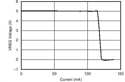
| VVREG | Output voltage | IOUT = 1 to 30 mA | 4.75 | 5 | 5.25 | V |
| IVREG | Output current | 30 | mA | |||
| VSW SUPPLY | ||||||
| RDS(ON) | VSW switch on-resistance | IOUT = 1 to 30 mA | 9 | 20 | Ω | |
| IVSW | Output current | 30 | mA | |||
| INTERNAL CLOCK OSCILLATOR | ||||||
| fCLK50 | Internal CLK50 clock frequency | 50 | MHz | |||
| LOGIC-LEVEL INPUTS AND OUTPUTS | ||||||
| VIL | Low-level input voltage | 0.8 | V | |||
| VIH | High-level input voltage | 1.5 | 5.5 | V | ||
| IIL | Low-level input current | –50 | 50 | µA | ||
| IIH | High-level input current | VIN = 3.3 V, DIR, BRAKE, PWM | 20 | 100 | µA | |
| VIN = 3.3 V, ENABLEn | 6 | 9 | ||||
| VHYS | Input hysteresis voltage | 0.1 | 0.3 | 0.5 | V | |
| RPD | Input pulldown resistance | DIR, BRAKE, PWM | 50 | 100 | 150 | kΩ |
| ENABLEn | 350 | 550 | ||||
| OPEN DRAIN OUTPUTS | ||||||
| VOL | Low-level output voltage | IOUT = 2.0 mA | 0.5 | V | ||
| IOH | Output leakage current | VOUT = 3.3 V | 1 | µA | ||
| HALL SENSOR INPUTS | ||||||
| VHYS | Hall amplifier hysteresis voltage | 15 | 20 | 25 | mV | |
| ∆VHYS | Hall amplifier hysteresis difference | Between U, V, W | –5 | 5 | mV | |
| VID | Hall amplifier input differential | 50 | mV | |||
| VCM | Hall amplifier input common mode voltage range | 1.5 | 3.5 | V | ||
| IIN | Input leakage current | Hx+ = Hx– | –10 | 10 | μA | |
| MOSFET DRIVERS | ||||||
| VOUTH | High-side gate drive output voltage | IO = 100 μA, VM ≥ 12V | VM + 10 | V | ||
| VOUTL | Low-side gate drive output voltage | IO = 100 μA | 10 | V | ||
| IOUT | Peak gate drive current | 30 | mA | |||
| CYCLE-BY-CYCLE CURRENT LIMITER | ||||||
| VLIMITER | Voltage limit across RISENSE for the current limiter | 0.225 | 0.25 | 0.275 | V | |
| PROTECTION CIRCUITS | ||||||
| VSENSEOCP | Voltage limit across RISENSE for overcurrent protection | 1.7 | 1.8 | 1.9 | V | |
| VFETOCP | Voltage limit across each external FET’s drain | 850 | 1000 | 1200 | mV | |
| VUVLO | VM undervoltage lockout | VM rising | 8 | V | ||
| VM falling | 7.8 | |||||
| VOVLO | VM overvoltage lockout | VM rising | 32 | 34 | 36 | V |
| TTSD | Thermal shutdown die temperature | 150 | 160 | °C | ||
| tLOCK | Locked rotor detect time | 3 | s | |||
| VCPFAIL | VCP failure threshold | VM + 3.0 | V | |||
6.6 Timing Requirements
| MIN | NOM | MAX | UNIT | |||
|---|---|---|---|---|---|---|
| HALL SENSOR INPUTS | ||||||
| tHDEG | Hall deglitch time | 20 | μs | |||
| CYCLE-BY-CYCLE CURRENT LIMITER | ||||||
| tBLANK | Time that VLIMITER is ignored, from the start of the PWM cycle | 6 | µs | |||
| PROTECTION CIRCUITS | ||||||
| tRETRY | Fault retry time after RLOCK or OTS | 5 | s | |||
| tSENSEOCP | Deglitch time for VSENSEOCP to trigger | 5 | µs | |||
| tFETOCP | Deglitch time for VFETOCP to trigger | 5 | µs | |||
6.7 Typical Characteristics


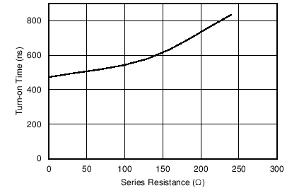
| With the CSD88537ND FETs, a series resistor was added to the | ||
| high-side gate drive, and the VGS rise time was measured. | ||