SLVSDZ9 May   2019 DRV8340-Q1

PRODUCTION DATA.  

  1. Features
  2. Applications
  3. Description
    1.     Simplified Schematic
  4. Revision History
  5. Device Comparison Table
  6. Pin Configuration and Functions
    1. Table 1. Pin Functions—DRV8340H
    2. Table 2. Pin Functions—DRV8340S
  7. Specifications
    1. 7.1 Absolute Maximum Ratings
    2. 7.2 ESD Ratings
    3. 7.3 Recommended Operating Conditions
    4. 7.4 Thermal Information
    5. 7.5 Electrical Characteristics
    6. 7.6 SPI Timing Requirements
    7. 7.7 Typical Characteristics
  8. Detailed Description
    1. 8.1 Overview
    2. 8.2 Functional Block Diagram
    3. 8.3 Feature Description
      1. 8.3.1 Three Phase Smart Gate Drivers
        1. 8.3.1.1 PWM Control Modes
          1. 8.3.1.1.1 6x PWM Mode (PWM_MODE = 000b or MODE Pin Tied to AGND)
          2. 8.3.1.1.2 3x PWM Mode (PWM_MODE = 001b or MODE Pin = 18 kΩ to AGND)
          3. 8.3.1.1.3 1x PWM Mode (PWM_MODE = 010b or MODE Pin = 75 kΩ to AGND)
          4. 8.3.1.1.4 Independent Half-Bridge PWM Mode (PWM_MODE = 011b or MODE Pin is > 1.5 MΩ to AGND or Hi-Z)
          5. 8.3.1.1.5 Phases A and B are Independent Half-Bridges, Phase C is Independent FET (MODE = 100b)
          6. 8.3.1.1.6 Phases B and C are Independent Half-Bridges, Phase A is Independent FET (MODE = 101b or MODE Pin is 75 kΩ to DVDD)
          7. 8.3.1.1.7 Phases A is Independent Half-Bridge, Phases B and C are Independent FET (MODE = 110b or MODE Pin is 18 kΩ to DVDD)
          8. 8.3.1.1.8 Independent MOSFET Drive Mode (PWM_MODE = 111b or MODE Pin = 0.47 kΩ to DVDD)
        2. 8.3.1.2 Device Interface Modes
          1. 8.3.1.2.1 Serial Peripheral Interface (SPI)
          2. 8.3.1.2.2 Hardware Interface
        3. 8.3.1.3 Gate Driver Voltage Supplies
        4. 8.3.1.4 Smart Gate Drive Architecture
          1. 8.3.1.4.1 IDRIVE: MOSFET Slew-Rate Control
          2. 8.3.1.4.2 TDRIVE: MOSFET Gate Drive Control
          3. 8.3.1.4.3 Propagation Delay
          4. 8.3.1.4.4 MOSFET VDS Monitors
          5. 8.3.1.4.5 VDRAIN Sense Pin
          6. 8.3.1.4.6 nFAULT Pin
      2. 8.3.2 DVDD Linear Voltage Regulator
      3. 8.3.3 Pin Diagrams
      4. 8.3.4 Gate Driver Protective Circuits
        1. 8.3.4.1 VM Supply Undervoltage Lockout (UVLO)
        2. 8.3.4.2 VCP Charge Pump Undervoltage Lockout (CPUV)
        3. 8.3.4.3 MOSFET VDS Overcurrent Protection (VDS_OCP)
          1. 8.3.4.3.1 VDS Latched Shutdown (OCP_MODE = 00b)
          2. 8.3.4.3.2 VDS Automatic Retry (OCP_MODE = 01b)
          3. 8.3.4.3.3 VDS Report Only (OCP_MODE = 10b)
          4. 8.3.4.3.4 VDS Disabled (OCP_MODE = 11b)
        4. 8.3.4.4 Gate Driver Fault (GDF)
        5. 8.3.4.5 Thermal Warning (OTW)
        6. 8.3.4.6 Thermal Shutdown (OTSD)
          1. 8.3.4.6.1 Latched Shutdown (OTSD_MODE = 0b)
          2. 8.3.4.6.2 Automatic Recovery (OTSD_MODE = 1b)
        7. 8.3.4.7 Open Load Detection (OLD)
          1. 8.3.4.7.1 Open Load Detection in Passive Mode (OLP)
            1. 8.3.4.7.1.1 OLP Steps
          2. 8.3.4.7.2 Open Load Detection in Active Mode (OLA)
        8. 8.3.4.8 Offline Shorts Diagnostics
          1. 8.3.4.8.1 Offline Short-to-Supply Diagnostic (SHT_BAT)
          2. 8.3.4.8.2 Offline Short-to-Ground Diagnostic (SHT_GND)
        9. 8.3.4.9 Reverse Supply Protection
    4. 8.4 Device Functional Modes
      1. 8.4.1 Gate Driver Functional Modes
        1. 8.4.1.1 Sleep Mode
        2. 8.4.1.2 Operating Mode
        3. 8.4.1.3 Fault Reset (CLR_FLT or ENABLE Reset Pulse)
    5. 8.5 Programming
      1. 8.5.1 SPI Communication
        1. 8.5.1.1 SPI
          1. 8.5.1.1.1 SPI Format
    6. 8.6 Register Maps
      1. 8.6.1 Status Registers
        1. 8.6.1.1 FAULT Status Register (Address = 0x00) [reset = 0x00]
          1. Table 17. FAULT Status Register Field Descriptions
        2. 8.6.1.2 DIAG Status A Register (Address = 0x01) [reset = 0x00]
          1. Table 18. DIAG Status A Register Field Descriptions
        3. 8.6.1.3 DIAG Status B Register (Address = 0x02) [reset = 0x00]
          1. Table 19. DIAG Status B Register Field Descriptions
        4. 8.6.1.4 DIAG Status C Register (address = 0x03) [reset = 0x00]
          1. Table 20. DIAG Status C Register Field Descriptions
      2. 8.6.2 Control Registers
        1. 8.6.2.1  IC1 Control Register (Address = 0x04) [reset = 0x00]
          1. Table 22. IC1 Control Field Descriptions
        2. 8.6.2.2  IC2 Control Register (address = 0x05) [reset = 0x40]
          1. Table 23. IC2 Control Field Descriptions
        3. 8.6.2.3  IC3 Control Register (Address = 0x06) [reset = 0xFF]
          1. Table 24. IC3 Control Field Descriptions
        4. 8.6.2.4  IC4 Control Register (Address = 0x07) [reset = 0xFF]
          1. Table 25. IC4 Control Field Descriptions
        5. 8.6.2.5  IC5 Control Register (Address = 0x08) [reset = 0xFF]
          1. Table 26. IC5 Control Field Descriptions
        6. 8.6.2.6  IC6 Control Register (Address = 0x09) [reset = 0x99]
          1. Table 27. IC6 Control Field Descriptions
        7. 8.6.2.7  IC7 Control Register (Address = 0x0A) [reset = 0x99]
          1. Table 28. IC7 Control Field Descriptions
        8. 8.6.2.8  IC8 Control Register (Address = 0x0B) [reset = 0x99]
          1. Table 29. IC8 Control Field Descriptions
        9. 8.6.2.9  IC9 Control Register (Address = 0x0C) [reset = 0x2F]
          1. Table 30. IC9 Control Field Descriptions
        10. 8.6.2.10 IC10 Control Register (Address = 0x0D) [reset = 0x61]
          1. Table 31. IC10 Control Field Descriptions
        11. 8.6.2.11 IC11 Control Register (Address = 0x0E) [reset = 0x00]
          1. Table 32. IC11 Control Field Descriptions
        12. 8.6.2.12 IC12 Control Register (Address = 0x0F) [reset = 0x2A]
          1. Table 33. IC12 Control Field Descriptions
        13. 8.6.2.13 IC13 Control Register (Address = 0x10) [reset = 0x7F]
          1. Table 34. IC13 Control Field Descriptions
        14. 8.6.2.14 IC14 Control Register (Address = 0x10) [reset = 0x00]
          1. Table 35. IC14 Control Field Descriptions
  9. Application and Implementation
    1. 9.1 Application Information
    2. 9.2 Typical Application
      1. 9.2.1 Primary Application
        1. 9.2.1.1 Design Requirements
        2. 9.2.1.2 Detailed Design Procedure
          1. 9.2.1.2.1 External MOSFET Support
            1. 9.2.1.2.1.1 Example
          2. 9.2.1.2.2 IDRIVE Configuration
            1. 9.2.1.2.2.1 Example
          3. 9.2.1.2.3 VDS Overcurrent Monitor Configuration
            1. 9.2.1.2.3.1 Example
          4. 9.2.1.2.4 Design consideration of low-side gate drive (IDRIVE, GLx, SLx)
          5. 9.2.1.2.5 External Components
        3. 9.2.1.3 Application Curves
  10. 10Power Supply Recommendations
    1. 10.1 Power Supply Consideration in Generator Mode
    2. 10.2 Bulk Capacitance Sizing
  11. 11Layout
    1. 11.1 Layout Guidelines
    2. 11.2 Layout Example
  12. 12Device and Documentation Support
    1. 12.1 Device Support
      1. 12.1.1 Device Nomenclature
    2. 12.2 Documentation Support
      1. 12.2.1 Related Documentation
    3. 12.3 Receiving Notification of Documentation Updates
    4. 12.4 Community Resources
    5. 12.5 Trademarks
    6. 12.6 Electrostatic Discharge Caution
    7. 12.7 Glossary
  13. 13Mechanical, Packaging, and Orderable Information

Package Options

Mechanical Data (Package|Pins)
Thermal pad, mechanical data (Package|Pins)
Orderable Information

OLP Steps

The OLP algorithm list is as follows:

  • The pullup current source is enabled. If a load is connected, current passes through the pullup resistor and the OLx_PU comparator output stays low. If an open load condition occurs, the current through the pullup resistor goes 0 and the OLx_PU comparator trips high.
  • The pulldown current source is enabled. In the same way, the OLx_PD comparator output either stays low to indicate load-connected, or trips high to indicate an open load condition.
  • If both the OLx_PU and OLx_PD comparators report an open load, the OL_PH_x bit in the SPI register latches high, and the nFAULT line goes low, to indicate an OL fault.

When the OL condition is removed, a clear faults command must be issued by the micro-controller either through the CLR_FLT bit or an ENABLE reset pulse which resets open load register bits. The charge pump stays active during this fault condition. The load connections shown in Figure 29 are not supported OLP.
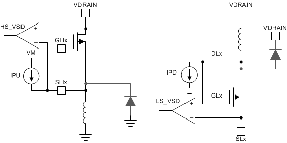
DRV8340-Q1 drv8343-q1-load-configurations-not-supported.gifFigure 29. Load Configurations Not Supported