SLVSFV1B August   2018  – August 2021 DRV8350F , DRV8353F

PRODUCTION DATA  

  1. Features
  2. Applications
  3. Description
  4. Revision History
  5. Device Comparison Table
  6. Pin Configuration and Functions
    1.     Pin Functions—32-Pin DRV8350F Devices
    2.     8
    3.     Pin Functions—40-Pin DRV8353F Devices
    4.     10
  7. Specifications
    1. 7.1 Absolute Maximum Ratings
    2. 7.2 ESD Ratings
    3. 7.3 Recommended Operating Conditions
    4. 7.4 Thermal Information
    5. 7.5 Electrical Characteristics
    6. 7.6 SPI Timing Requirements
    7. 7.7 Typical Characteristics
  8. Detailed Description
    1. 8.1 Overview
    2. 8.2 Functional Block Diagram
    3. 8.3 Feature Description
      1. 8.3.1 Three Phase Smart Gate Drivers
        1. 8.3.1.1 PWM Control Modes
          1. 8.3.1.1.1 6x PWM Mode (PWM_MODE = 00b or MODE Pin Tied to AGND)
          2. 8.3.1.1.2 3x PWM Mode (PWM_MODE = 01b or MODE Pin = 47 kΩ to AGND)
          3. 8.3.1.1.3 1x PWM Mode (PWM_MODE = 10b or MODE Pin = Hi-Z)
          4. 8.3.1.1.4 Independent PWM Mode (PWM_MODE = 11b or MODE Pin Tied to DVDD)
        2. 8.3.1.2 Device Interface Modes
          1. 8.3.1.2.1 Serial Peripheral Interface (SPI)
          2. 8.3.1.2.2 Hardware Interface
        3. 8.3.1.3 Gate Driver Voltage Supplies and Input Supply Configurations
        4. 8.3.1.4 Smart Gate Drive Architecture
          1. 8.3.1.4.1 IDRIVE: MOSFET Slew-Rate Control
          2. 8.3.1.4.2 TDRIVE: MOSFET Gate Drive Control
          3. 8.3.1.4.3 Propagation Delay
          4. 8.3.1.4.4 MOSFET VDS Monitors
          5. 8.3.1.4.5 VDRAIN Sense and Reference Pin
      2. 8.3.2 DVDD Linear Voltage Regulator
      3. 8.3.3 Pin Diagrams
      4. 8.3.4 Low-Side Current-Shunt Amplifiers (DRV8353F)
        1. 8.3.4.1 Bidirectional Current Sense Operation
        2. 8.3.4.2 Unidirectional Current Sense Operation (SPI only)
        3. 8.3.4.3 Amplifier Calibration Modes
        4. 8.3.4.4 MOSFET VDS Sense Mode (SPI Only)
      5. 8.3.5 Gate Driver Protective Circuits
        1. 8.3.5.1 VM Supply and VDRAIN Undervoltage Lockout (UVLO)
        2. 8.3.5.2 VCP Charge-Pump and VGLS Regulator Undervoltage Lockout (GDUV)
        3. 8.3.5.3 MOSFET VDS Overcurrent Protection (VDS_OCP)
          1. 8.3.5.3.1 VDS Latched Shutdown (OCP_MODE = 00b)
          2. 8.3.5.3.2 VDS Automatic Retry (OCP_MODE = 01b)
          3. 8.3.5.3.3 VDS Report Only (OCP_MODE = 10b)
          4. 8.3.5.3.4 VDS Disabled (OCP_MODE = 11b)
        4. 8.3.5.4 VSENSE Overcurrent Protection (SEN_OCP)
          1. 8.3.5.4.1 VSENSE Latched Shutdown (OCP_MODE = 00b)
          2. 8.3.5.4.2 VSENSE Automatic Retry (OCP_MODE = 01b)
          3. 8.3.5.4.3 VSENSE Report Only (OCP_MODE = 10b)
          4. 8.3.5.4.4 VSENSE Disabled (OCP_MODE = 11b or DIS_SEN = 1b)
        5. 8.3.5.5 Gate Driver Fault (GDF)
        6. 8.3.5.6 Overcurrent Soft Shutdown (OCP Soft)
        7. 8.3.5.7 Thermal Warning (OTW)
        8. 8.3.5.8 Thermal Shutdown (OTSD)
        9. 8.3.5.9 Fault Response Table
    4. 8.4 Device Functional Modes
      1. 8.4.1 Gate Driver Functional Modes
        1. 8.4.1.1 Sleep Mode
        2. 8.4.1.2 Operating Mode
        3. 8.4.1.3 Fault Reset (CLR_FLT or ENABLE Reset Pulse)
    5. 8.5 Programming
      1. 8.5.1 SPI Communication
        1. 8.5.1.1 SPI
          1. 8.5.1.1.1 SPI Format
    6. 8.6 Register Maps
      1. 8.6.1 Status Registers
        1. 8.6.1.1 Fault Status Register 1 (address = 0x00h)
        2. 8.6.1.2 Fault Status Register 2 (address = 0x01h)
      2. 8.6.2 Control Registers
        1. 8.6.2.1 Driver Control Register (address = 0x02h)
        2. 8.6.2.2 Gate Drive HS Register (address = 0x03h)
        3. 8.6.2.3 Gate Drive LS Register (address = 0x04h)
        4. 8.6.2.4 OCP Control Register (address = 0x05h)
        5. 8.6.2.5 CSA Control Register (DRV8353FOnly) (address = 0x06h)
        6. 8.6.2.6 Driver Configuration Register (DRV8353F Only) (address = 0x07h)
  9. Application and Implementation
    1. 9.1 Application Information
    2. 9.2 Typical Application
      1. 9.2.1 Primary Application
        1. 9.2.1.1 Design Requirements
        2. 9.2.1.2 Detailed Design Procedure
          1. 9.2.1.2.1 External MOSFET Support
            1. 9.2.1.2.1.1 MOSFET Example
          2. 9.2.1.2.2 IDRIVE Configuration
            1. 9.2.1.2.2.1 IDRIVE Example
          3. 9.2.1.2.3 VDS Overcurrent Monitor Configuration
            1. 9.2.1.2.3.1 VDS Overcurrent Example
          4. 9.2.1.2.4 Sense-Amplifier Bidirectional Configuration (DRV8353F)
            1. 9.2.1.2.4.1 Sense-Amplifier Example
          5. 9.2.1.2.5 Single Supply Power Dissipation
          6. 9.2.1.2.6 Single Supply Power Dissipation Example
        3. 9.2.1.3 Application Curves
      2. 9.2.2 Alternative Application
        1. 9.2.2.1 Design Requirements
        2. 9.2.2.2 Detailed Design Procedure
          1. 9.2.2.2.1 Sense Amplifier Unidirectional Configuration
            1. 9.2.2.2.1.1 Sense-Amplifier Example
            2. 9.2.2.2.1.2 Dual Supply Power Dissipation
            3. 9.2.2.2.1.3 Dual Supply Power Dissipation Example
  10. 10Power Supply Recommendations
    1. 10.1 Bulk Capacitance Sizing
  11. 11Layout
    1. 11.1 Layout Guidelines
    2. 11.2 Layout Example
  12. 12Device and Documentation Support
    1. 12.1 Device Support
      1. 12.1.1 Device Nomenclature
    2. 12.2 Documentation Support
      1. 12.2.1 Related Documentation
    3. 12.3 Related Links
    4. 12.4 Receiving Notification of Documentation Updates
    5. 12.5 Support Resources
    6. 12.6 Trademarks
    7. 12.7 Electrostatic Discharge Caution
    8. 12.8 Glossary
  13. 13Mechanical, Packaging, and Orderable Information

Package Options

Mechanical Data (Package|Pins)
Thermal pad, mechanical data (Package|Pins)
Orderable Information
Sense Amplifier Unidirectional Configuration

The sense amplifiers are configured to be unidirectional through the registers on SPI devices by writing a 0 to the VREF_DIV bit.

The sense-amplifier gain and sense resistor values are selected based on the target current range, VREF, sense-resistor power rating, and operating temperature range. In unidirectional operation of the sense amplifier, use Equation 31 to calculate the approximate value of the dynamic range at the output.

Equation 31. GUID-87A672D4-31FA-46D7-8453-E73854F4504E-low.gif

Use Equation 32 to calculate the approximate value of the selected sense resistor.
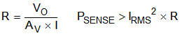
Equation 32. GUID-43AE54A3-0C11-4557-92C5-FE1074260CBA-low.gif

where

  • GUID-96BDD209-F0AD-4632-82F6-AC9D5C5A1E97-low.gif

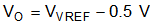
From Equation 31 and Equation 32, select a target gain setting based on the power rating of a target sense resistor.