SLVSFO2 July 2020 – MONTH DRV8353M
PRODUCTION DATA
- 1 Features
- 2 Applications
- 3 Description
- 4 Revision History
- 5 Device Comparison Table
- 6 Pin Configuration and Functions
- 7 Absolute Maximum Ratings
- 8 ESD Ratings
- 9 Recommended Operating Conditions
- 10Thermal Information
- 11Electrical Characteristics
- 12SPI Timing Requirements
-
13Detailed Description
- 13.1 Overview
- 13.2 Functional Block Diagram
- 13.3
Feature Description
- 13.3.1 Three Phase Smart Gate Drivers
- 13.3.2 DVDD Linear Voltage Regulator
- 13.3.3 Pin Diagrams
- 13.3.4 Low-Side Current-Shunt Amplifiers
- 13.3.5
Gate Driver Protective Circuits
- 13.3.5.1 VM Supply and VDRAIN Undervoltage Lockout (UVLO)
- 13.3.5.2 VCP Charge-Pump and VGLS Regulator Undervoltage Lockout (GDUV)
- 13.3.5.3 MOSFET VDS Overcurrent Protection (VDS_OCP)
- 13.3.5.4 VSENSE Overcurrent Protection (SEN_OCP)
- 13.3.5.5 Gate Driver Fault (GDF)
- 13.3.5.6 Overcurrent Soft Shutdown (OCP Soft)
- 13.3.5.7 Thermal Warning (OTW)
- 13.3.5.8 Thermal Shutdown (OTSD)
- 13.3.5.9 Fault Response Table
- 13.4 Device Functional Modes
- 13.5 Programming
- 13.6
Register Maps
- 13.6.1 Status Registers
- 13.6.2
Control Registers
- 13.6.2.1 Driver Control Register (address = 0x02h)
- 13.6.2.2 Gate Drive HS Register (address = 0x03h)
- 13.6.2.3 Gate Drive LS Register (address = 0x04h)
- 13.6.2.4 OCP Control Register (address = 0x05h)
- 13.6.2.5 CSA Control Register (address = 0x06h)
- 13.6.2.6 Driver Configuration Register (address = 0x07h)
-
14Application and Implementation
- 14.1 Application Information
- 14.2
Typical Application
- 14.2.1
Primary Application
- 14.2.1.1 Design Requirements
- 14.2.1.2 Detailed Design Procedure
- 14.2.1.3 Application Curves
- 14.2.1
Primary Application
- 15Power Supply Recommendations
- 16Layout
- 17Device and Documentation Support
- 18Mechanical, Packaging, and Orderable Information
Package Options
Mechanical Data (Package|Pins)
- RTA|40
Thermal pad, mechanical data (Package|Pins)
- RTA|40
Orderable Information
3 Description
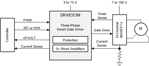
The DRV8353M family of devices are highly-integrated gate drivers for three-phase brushless DC (BLDC) motor applications. These applications include field-oriented control (FOC), sinusoidal current control, and trapezoidal current control of BLDC motors. The device variants provide optional integrated current shunt amplifiers to support different motor control schemes and a buck regulator to power the gate driver or external controller.
The DRV8353M uses smart gate drive (SGD) architecture to decrease the number of external components that are typically necessary for MOSFET slew rate control and protection circuits. The SGD architecture also optimizes dead time to prevent shoot-through conditions, provides flexibility in decreasing electromagnetic interference (EMI) by MOSFET slew rate control, and protects against gate short circuit conditions through VGS monitors. A strong gate pulldown circuit helps prevent unwanted dV/dt parasitic gate turn on events
Various PWM control modes (6x, 3x, 1x, and independent) are supported for simple interfacing to the external controller. These modes can decrease the number of outputs required of the controller for the motor driver PWM control signals. This family of devices also includes 1x PWM mode for simple sensored trapezoidal control of a BLDC motor by using an internal block commutation table.
| PART NUMBER | PACKAGE | BODY SIZE (NOM) |
|---|---|---|
| DRV8353M | WQFN (40) | 6.00 mm x 6.00 mm |
- For all available packages, see the orderable addendum at the end of the data sheet.
 Simplified Schematic