SLOS629D July   2010  – October 2016 DRV8601

PRODUCTION DATA.  

  1. Features
  2. Applications
  3. Description
  4. Revision History
  5. Pin Configuration and Functions
  6. Specifications
    1. 6.1 Absolute Maximum Ratings
    2. 6.2 ESD Ratings
    3. 6.3 Recommended Operating Conditions
    4. 6.4 Thermal Information
    5. 6.5 Electrical Characteristics
    6. 6.6 Operating Characteristics
    7. 6.7 Typical Characteristics
  7. Detailed Description
    1. 7.1 Overview
    2. 7.2 Functional Block Diagram
    3. 7.3 Feature Description
      1. 7.3.1 Support for ERM and LRA Actuators
      2. 7.3.2 Internal Reference
      3. 7.3.3 Shutdown Mode
    4. 7.4 Device Functional Modes
  8. Application and Implementation
    1. 8.1 Application Information
    2. 8.2 Typical Applications
      1. 8.2.1 Pseudo-Differential Feedback with Internal Reference
        1. 8.2.1.1 Design Requirements
        2. 8.2.1.2 Detailed Design Procedure
        3. 8.2.1.3 Application Curves
      2. 8.2.2 Pseudo-Differential Feedback with Level-Shifter
        1. 8.2.2.1 Design Requirements
        2. 8.2.2.2 Detailed Design Procedure
      3. 8.2.3 Differential Feedback With External Reference
        1. 8.2.3.1 Design Requirements
        2. 8.2.3.2 Detailed Design Procedure
          1. 8.2.3.2.1 Selecting Components
            1. 8.2.3.2.1.1 Resistors RI and RF
            2. 8.2.3.2.1.2 Capacitor CR
  9. Power Supply Recommendations
  10. 10Layout
    1. 10.1 Layout Guidelines
    2. 10.2 Layout Example
  11. 11Device and Documentation Support
    1. 11.1 Receiving Notification of Documentation Updates
    2. 11.2 Community Resources
    3. 11.3 Trademarks
    4. 11.4 Electrostatic Discharge Caution
    5. 11.5 Glossary
  12. 12Mechanical, Packaging, and Orderable Information

Package Options

Mechanical Data (Package|Pins)
Thermal pad, mechanical data (Package|Pins)
Orderable Information

10 Layout

10.1 Layout Guidelines

Use the following guidelines for the DRV8601 layout:

  • The decoupling capacitor for the power supply (VDD) should be placed closed to the device pin.
  • The REFOUT capacitor should be placed close to the device REFOUT pin.

10.2 Layout Example

Figure 19 shows a typical example of the layout for DRV8601. It is important that the power supply decoupling caps and the REFOUT external capacitance be connected as close to the device as possible.
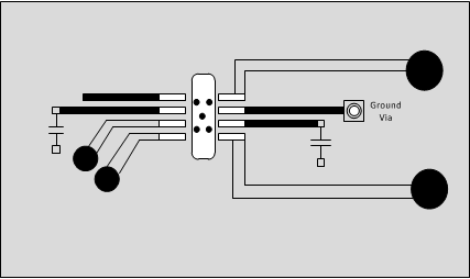
DRV8601 layout_SLOS269.gif Figure 19. Typical Layout Example
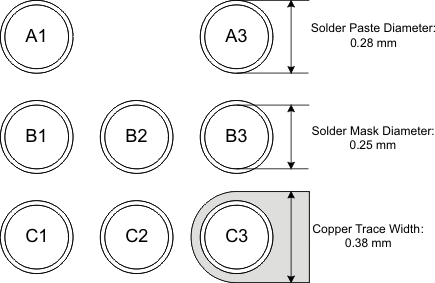
DRV8601 ZGV_land_los629.gif Figure 20. ZQV Land Pattern