SLOS629D July   2010  – October 2016 DRV8601

PRODUCTION DATA.  

  1. Features
  2. Applications
  3. Description
  4. Revision History
  5. Pin Configuration and Functions
  6. Specifications
    1. 6.1 Absolute Maximum Ratings
    2. 6.2 ESD Ratings
    3. 6.3 Recommended Operating Conditions
    4. 6.4 Thermal Information
    5. 6.5 Electrical Characteristics
    6. 6.6 Operating Characteristics
    7. 6.7 Typical Characteristics
  7. Detailed Description
    1. 7.1 Overview
    2. 7.2 Functional Block Diagram
    3. 7.3 Feature Description
      1. 7.3.1 Support for ERM and LRA Actuators
      2. 7.3.2 Internal Reference
      3. 7.3.3 Shutdown Mode
    4. 7.4 Device Functional Modes
  8. Application and Implementation
    1. 8.1 Application Information
    2. 8.2 Typical Applications
      1. 8.2.1 Pseudo-Differential Feedback with Internal Reference
        1. 8.2.1.1 Design Requirements
        2. 8.2.1.2 Detailed Design Procedure
        3. 8.2.1.3 Application Curves
      2. 8.2.2 Pseudo-Differential Feedback with Level-Shifter
        1. 8.2.2.1 Design Requirements
        2. 8.2.2.2 Detailed Design Procedure
      3. 8.2.3 Differential Feedback With External Reference
        1. 8.2.3.1 Design Requirements
        2. 8.2.3.2 Detailed Design Procedure
          1. 8.2.3.2.1 Selecting Components
            1. 8.2.3.2.1.1 Resistors RI and RF
            2. 8.2.3.2.1.2 Capacitor CR
  9. Power Supply Recommendations
  10. 10Layout
    1. 10.1 Layout Guidelines
    2. 10.2 Layout Example
  11. 11Device and Documentation Support
    1. 11.1 Receiving Notification of Documentation Updates
    2. 11.2 Community Resources
    3. 11.3 Trademarks
    4. 11.4 Electrostatic Discharge Caution
    5. 11.5 Glossary
  12. 12Mechanical, Packaging, and Orderable Information

Package Options

Mechanical Data (Package|Pins)
Thermal pad, mechanical data (Package|Pins)
Orderable Information

5 Pin Configuration and Functions

DRB Package
8-Pin VQFN
Top View
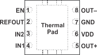
DRV8601 po_drb_pckg_top_slos629.gif
ZQV Package
8-Ball
Top View
DRV8601 ZQV_slos629.gif

Pin Functions

PIN TYPE(1) DESCRIPTION
NAME DRB
NO.
ZQV
NO.
EN 1 B1 I Chip enable
GND 7 B2 P Ground
IN1 4 C3 I Input to driver
IN2 3 C2 I Input to driver
OUT+ 5 B3 O Positive output
OUT– 8 A1 O Negative output
REFOUT 2 C1 O Reference voltage output
VDD 6 A3 P Supply voltage
(1) I = Input, O = Output, P = Power