SLVSAS7D February   2011  – March 2021 DRV8801-Q1

PRODUCTION DATA  

  1. Features
  2. Applications
  3. Description
  4. Revision History
  5. Pin Configuration and Functions
  6. Specifications
    1. 6.1 Absolute Maximum Ratings
    2. 6.2 ESD Ratings
    3. 6.3 Recommended Operating Conditions
    4. 6.4 Thermal Information
    5. 6.5 Electrical Characteristics
    6. 6.6 Timing Requirements
    7. 6.7 Typical Characteristics
  7. Detailed Description
    1. 7.1 Overview
    2. 7.2 Functional Block Diagram
    3. 7.3 Feature Description
      1. 7.3.1 Power Supervisor
      2. 7.3.2 Bridge Control
        1. 7.3.2.1 MODE 1
        2. 7.3.2.2 MODE 2
      3. 7.3.3 Fast Decay with Synchronous Rectification
      4. 7.3.4 Slow Decay with Synchronous Rectification (Brake Mode)
      5. 7.3.5 Charge Pump
      6. 7.3.6 SENSE
      7. 7.3.7 VPROPI
        1. 7.3.7.1 Connecting VPROPI Output to ADC
      8. 7.3.8 Protection Circuits
        1. 7.3.8.1 VBB Undervoltage Lockout (UVLO)
        2. 7.3.8.2 Overcurrent Protection (OCP)
        3. 7.3.8.3 Overtemperature Warning (OTW)
        4. 7.3.8.4 Overtemperature Shutdown (OTS)
      9. 7.3.9 Thermal Shutdown (TSD)
    4. 7.4 Device Functional Modes
  8. Application and Implementation
    1. 8.1 Application Information
    2. 8.2 Typical Application
      1. 8.2.1 Design Requirements
      2. 8.2.2 Detailed Design Procedure
        1. 8.2.2.1 Motor Voltage
        2. 8.2.2.2 Power Dissipation
        3. 8.2.2.3 Thermal Considerations
          1. 8.2.2.3.1 Junction-to-Ambiant Thermal Impedance (ƟJA)
        4. 8.2.2.4 Motor Current Trip Point
        5. 8.2.2.5 Sense Resistor Selection
        6. 8.2.2.6 Drive Current
      3. 8.2.3 Pulse-Width Modulating
        1. 8.2.3.1 Pulse-Width Modulating ENABLE
        2. 8.2.3.2 Pulse-Width Modulating PHASE
      4. 8.2.4 Application Curves
    3. 8.3 Parallel Configuration
      1. 8.3.1 Parallel Connections
      2. 8.3.2 Non – Parallel Connections
      3. 8.3.3 Wiring nFAULT as Wired OR
      4. 8.3.4 Electrical Considerations
        1. 8.3.4.1 Device Spacing
        2. 8.3.4.2 Recirculation Current Handling
        3. 8.3.4.3 Sense Resistor Selection
        4. 8.3.4.4 Maximum System Current
  9. Power Supply Recommendations
    1. 9.1 Bulk Capacitance
  10. 10Layout
    1. 10.1 Layout Guidelines
    2. 10.2 Layout Example
  11. 11Device and Documentation Support
    1. 11.1 Documentation Support
      1. 11.1.1 Related Documentation
    2. 11.2 Receiving Notification of Documentation Updates
    3. 11.3 Support Resources
    4. 11.4 Trademarks
    5. 11.5 Electrostatic Discharge Caution
    6. 11.6 Glossary
  12. 12Mechanical, Packaging, and Orderable Information

Package Options

Mechanical Data (Package|Pins)
Thermal pad, mechanical data (Package|Pins)
Orderable Information

SENSE

A low-value SENSE resistor is used to set an overcurrent threshold lower than the default maximum value of 2.8 A and to provide a voltage for VPROPI. This SENSE resistor must be connected between the SENSE pin and ground. To minimize ground-trace IR drops in sensing the output current level, the current-sensing resistor should have an independent ground return to the star ground point. This trace should be as short as possible. For low-value sense resistors, the IR drops in the PCB can be significant, and should be taken into account.

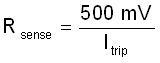
A direction connection to ground yields a SENSE voltage equal to zero. In that case, maximum current is 2.8 A and VPROPI outputs 0 V. A resistor connected as explained before, will yield a VPROPI output as detailed in the Section 7.3.7. Size the sense resistor such that voltage drop across the sense resistor is less than 500mV under normal loading conditions. Any voltage equal or larger to 500 mV will signal the device to hi-Z the H-bridge output as overcurrent trip threshold has been reached. In this case, device will enter recirculation as stipulated by the MODE input pin. The device automatically retries with a period of t(OCP).

Equation 1 shows the value of the resistor to a particular current setting.

Equation 1. GUID-20201203-CA0I-PT90-KQTM-278ZGBD1HRF2-low.gif

The overcurrent trip level selected cannot be greater than I(OCP).

GUID-88414B5B-1CB0-461A-8441-455EBB50781C-low.gifFigure 7-2 Overcurrent Control Timing