SLVSCI2A June 2014 – June 2014 DRV8802-Q1
PRODUCTION DATA.
- 1 Features
- 2 Applications
- 3 Description
- 4 Revision History
- 5 Pin Configuration and Functions
- 6 Specifications
- 7 Detailed Description
- 8 Application and Implementation
- 9 Power Supply Recommendations
- 10Layout
- 11Device and Documentation Support
- 12Mechanical, Packaging, and Orderable Information
Package Options
Mechanical Data (Package|Pins)
- PWP|28
Thermal pad, mechanical data (Package|Pins)
- PWP|28
Orderable Information
7 Detailed Description
7.1 Overview
The DRV8802-Q1 device provides an integrated motor driver solution for automotive applications. The device has two H-bridge drivers, and is intended to drive DC motors. The output driver block for each consists of N-channel power MOSFET’s configured as H-bridges to drive the motor windings. The DRV8802-Q1 device can supply up to 1.6-A peak or 1.1-A RMS output current (with proper heatsinking at 24 V and 25°C) per H-bridge. A simple parallel digital control interface is compatible with industry-standard devices. Decay mode is programmable to allow braking or coasting of the motor when disabled. Internal shutdown functions are provided for over current protection, short circuit protection, under voltage lockout and overtemperature.
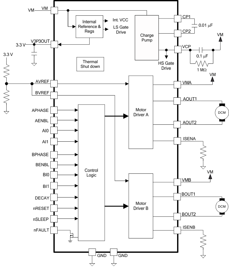
7.2 Functional Block Diagram
7.3 Feature Description
7.3.1 PWM Motor Drivers
The DRV8802-Q1 device contains two H-bridge motor drivers with current-control PWM circuitry. Figure 5 shows a block diagram of the motor control circuitry.
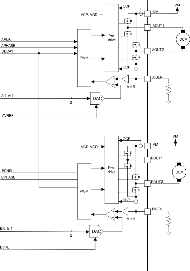 Figure 5. Motor Control Circuitry
Note that there are multiple VM pins (VMx). All VMx pins must be connected together to the motor supply voltage.
7.3.2 Bridge Control
The xPHASE input pins control the direction of current flow through each H-bridge, and therefore control the direction of rotation of a DC motor. The xENBL input pins enable the H-bridge outputs when active high, and can also be used for PWM speed control of the motor. Table 1 lists the H-bridge logic.
Table 1. H-Bridge Logic
| xENBL | xPHASE | xOUT1 | xOUT2 |
|---|---|---|---|
| 0 | X | see (1) | see (1) |
| 1 | 1 | H | L |
| 1 | 0 | L | H |
7.3.3 Current Regulation
The current through the motor windings is regulated by a fixed-frequency PWM current regulation, or current chopping. When an H-bridge is enabled, current rises through the winding at a rate dependent on the DC voltage and inductance of the winding. When the current hits the current chopping threshold, the bridge disables the current until the beginning of the next PWM cycle.
For stepping motors, current regulation is normally used at all times, and can change the current that is used to microstep the motor. For DC motors, current regulation is used to limit the start-up and stall current of the motor.
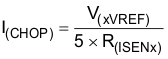
The PWM chopping current is set by a comparator that compares the voltage across a current sense resistor connected to the xISEN pins, multiplied by a factor of 5, with a reference voltage. The reference voltage is input from the xVREF pins, and is scaled by a 2-bit DAC that allows current settings of 38%, 71%, and 100% of full-scale, plus zero.
Use Equation 1 to calculate the full-scale (100%) chopping current.
For example:
If a 0.5-Ω sense resistor is used and the voltage on the xVREF pin is 3.3 V, the full-scale (100%) chopping current is 3.3 V / (5 × 0.5 Ω) = 1.32 A.
Two input pins per H-bridge (xI1 and xI0) are used to scale the current in each bridge as a percentage of the full-scale current set by the xVREF input pin and sense resistance. Table 2 lists the function of the pins.
Table 2. H-Bridge Pin Functions
| xI1 | xI0 | RELATIVE CURRENT (% FULL-SCALE CHOPPING CURRENT) |
|---|---|---|
| 1 | 1 | 0% (Bridge disabled) |
| 1 | 0 | 38% |
| 0 | 1 | 71% |
| 0 | 0 | 100% |
Note that when both xI bits are 1, the H-bridge is disabled and no current flows.
For example:
If a 0.5-Ω sense resistor is used and the voltage on the xVREF pin is 3.3 V, the chopping current is 1.32 A at the 100% setting (xI1, xI0 = 00). At the 71% setting (xI1, xI0 = 01) the current is 1.32 A × 0.71 = 0.937 A. At the 38% setting (xI1, xI0 = 10) the current is 1.32 A × 0.38 = 0.502 A. If (xI1, xI0 = 11) the bridge is disabled and no current will flow.
7.3.4 Decay Mode and Braking
During PWM current chopping, the H-bridge is enabled to drive current through the motor winding until the PWM current chopping threshold is reached. See case 1 in Figure 6. The current-flow direction shown indicates the state when the xENBL pin is high.
When the chopping current threshold is reached, the H-bridge can operate in two different states, fast decay or slow decay.
In fast decay mode, when the PWM chopping current level has been reached, the H-bridge reverses state to allow winding current to flow in a reverse direction. As the winding current approaches zero, the bridge is disabled to prevent any reverse current flow. See case 2 in Figure 6 for fast decay mode.
In slow decay mode, winding current is re-circulated by enabling both of the low-side FETs in the bridge. See case 3 in Figure 6.
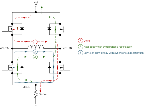 Figure 6. Decay Mode
The DRV8802-Q1 device supports fast decay and slow decay mode. Slow or fast decay mode is selected by the state of the DECAY pin. A logic low selects slow decay, and logic high sets fast decay mode. Note that the DECAY pin sets the decay mode for both H-bridges.
The DECAY mode also affects the operation of the bridge when it is disabled (by taking the ENBL pin inactive). This effect applies if the ENABLE input is being used for PWM speed control of the motor, or if it is simply being used to start and stop motor rotation.
If the DECAY pin is high (fast decay), when the bridge is disabled, all FETs are turned off and decay current flows through the body diodes, allowing the motor to coast to a stop.
If the DECAY pin is low (slow decay), both low-side FETs are turned on when the xENBL pin is made inactive. When the xENBL pin is made inactive, the inactivation essentially shorts out the back EMF of the motor, causing the motor to brake, and stop quickly. The low-side FETs stays in the ON state even after the current reaches zero.
7.3.5 Blanking Time
After the current is enabled in an H-bridge, the voltage on the xISEN pin is ignored for a fixed period of time before enabling the current sense circuitry. This blanking time is fixed at 3.75 μs. Note that the blanking time also sets the minimum on time of the PWM.
7.3.6 nRESET and nSLEEP Operation
The nRESET pin, when driven active low, resets the internal logic. This pin also disables the H-bridge drivers. All inputs are ignored while nRESET is active.
Driving nSLEEP low puts the device into a low power sleep state. In this state, the H-bridges are disabled, the gate drive charge pump is stopped, the V3P3OUT regulator is disabled, and all internal clocks are stopped. In this state all inputs are ignored until nSLEEP returns inactive high. When returning from sleep mode, some time (approximately 1 ms) must pass before the motor driver becomes fully operational.
7.3.7 Protection Circuits
The DRV8802-Q1 device is fully protected against undervoltage, overcurrent, and overtemperature events.
| FAULT | ERROR REPORT | H-BRIDGE | CHARGE PUMP | RECOVERY |
|---|---|---|---|---|
| V(VMx) undervoltage (UVLO) | No error report – nFAULT is hi-Z | Disabled | Shut Down | V(VMx) > VUVLO RISING |
| Overcurrent (OCP) | nFAULT pulled low | Disabled | Operating | Retry time, t(OCP) |
| Overtemperature Shutdown (OTS) | nFAULT remains pulled low (set during OTW) | Disabled | Shut Down | TJ < T(OTS) – Thys(OTS) |
7.3.7.1 Overcurrent Protection (OCP)
An analog current-limit circuit on each FET limits the current through the FET by removing the gate drive. If this analog current-limit persists for longer than the OCP time, all FETs in the H-bridge are disabled and the nFAULT pin is driven low. The device remains disabled until either nRESET pin is applied, or V(VMx) is removed and re-applied.
Overcurrent conditions on both high-side and low-side devices (such as a short to ground, supply, or across the motor winding) result in an overcurrent shutdown. Note that overcurrent protection does not use the current sense circuitry used for PWM current control and is independent of the R(ISENx) resistor value or xVREF voltage.
7.3.7.2 Thermal Shutdown (TSD)
If the die temperature exceeds the thermal shutdown temperature limit, all FETs in the H-bridge are disabled and the nFAULT pin is driven low. When the die temperature has fallen below the temperature hsyteresis level, operation resumes automatically.
7.3.7.3 Undervoltage Lockout (UVLO)
If at any time the voltage on the VMx pins falls below the undervoltage lockout threshold voltage, all circuitry in the device is disabled and internal logic resets. Operation resumes when VM rises above the UVLO threshold.
7.4 Device Functional Modes
The DRV8802-Q1 device is active unless the nSLEEP pin is brought logic low. In sleep mode the charge pump is disabled, the V3P3OUT regulator is disabled, and the H-bridge FETs are disabled hi-Z. The DRV8802-Q1 is brought out of sleep mode when nSLEEP is brought logic high.