SLVSCI2A June 2014 – June 2014 DRV8802-Q1
PRODUCTION DATA.
- 1 Features
- 2 Applications
- 3 Description
- 4 Revision History
- 5 Pin Configuration and Functions
- 6 Specifications
- 7 Detailed Description
- 8 Application and Implementation
- 9 Power Supply Recommendations
- 10Layout
- 11Device and Documentation Support
- 12Mechanical, Packaging, and Orderable Information
Package Options
Mechanical Data (Package|Pins)
- PWP|28
Thermal pad, mechanical data (Package|Pins)
- PWP|28
Orderable Information
10 Layout
10.1 Layout Guidelines
The VMA and VMB pins should be bypassed to GND using low-ESR ceramic bypass capacitors with a recommended value of 0.1-μF rated for VM. This capacitor should be placed as close to the VMA and VMB pins as possible with a thick trace or ground plane connection to the device GND pin. The VMA and VMB pins must be bypassed to ground using an appropriate bulk capacitor. This component may be an electrolytic and should be located close to the DRV8802-Q1. A low-ESR ceramic capacitor must be placed in between the CPL and CPH pins. TI recommends a value of 0.01-μF rated for VM. Place this component as close to the pins as possible. A low-ESR ceramic capacitor must be placed in between the VMA and VCP pins. TI recommends a value of 0.1-μF rated for 16 V. Place this component as close to the pins as possible. Also, place a 1-MΩ resistor between VCP and VMA. Bypass V3P3 to ground with a ceramic capacitor rated 6.3 V. Place this bypass capacitor as close to the pin as possible.
10.2 Layout Example
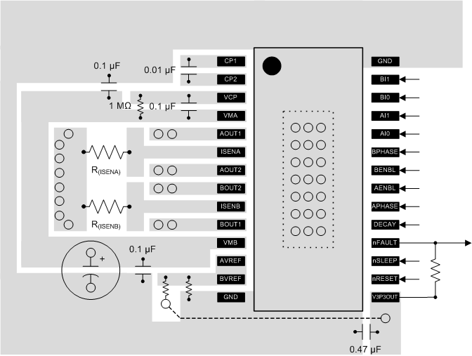 Figure 11. DRV8802-Q1 Layout Example
10.3 Thermal Information
10.3.1 Thermal Protection
The DRV8802-Q1 device has thermal shutdown (TSD) as described in the Thermal Shutdown (TSD) section. If the die temperature exceeds approximately 150°C, the device is disabled until the temperature drops below the hysteresis level.
Any tendency of the device to enter TSD is an indication of either excessive power dissipation, insufficient heatsinking, or too high an ambient temperature.
10.3.2 Power Dissipation
Power dissipation in the DRV8802-Q1 device is dominated by the power dissipated in the output FET resistance, or rDS(on). Use Equation 4 to calculate the estimated average power dissipation of each H-bridge when running a DC motor.
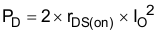
where
- PD is the power dissipation of one H-bridge
- rDS(on) is the resistance of each FET
- IO is the RMS output current being applied to each winding
IO is equal to the average current drawn by the DC motor. Note that at startup and fault conditions this current is much higher than normal running current; these peak currents and the current duration must also be considered. The factor of 2 exists because at any instant two FETs are conducting winding current (one high-side and one low-side).
The total device dissipation is the power dissipated in each of the two H-bridges added together.
The maximum amount of power that can be dissipated in the device is dependent on ambient temperature and heatsinking.
NOTE
rDS(on) increases with temperature, so as the device heats, the power dissipation increases. This fact must be taken into consideration when sizing the heatsink.
10.3.3 Heatsinking
The PowerPAD package uses an exposed pad to remove heat from the device. For proper operation, this pad must be thermally connected to copper on the PCB to dissipate heat. On a multi-layer PCB with a ground plane, this connection can be accomplished by adding a number of vias to connect the thermal pad to the ground plane. On PCBs without internal planes, a copper area can be added on either side of the PCB to dissipate heat. If the copper area is on the opposite side of the PCB from the device, thermal vias are used to transfer the heat between top and bottom layers.
For details about how to design the PCB, refer to the TI application report, PowerPAD™ Thermally Enhanced Package (SLMA002), "" and the TI application brief, PowerPAD Made Easy™ (SLMA004), available at www.ti.com.
In general, the more copper area that can be provided, the more power can be dissipated.