SLVSCH0 April 2014 DRV8824-Q1
PRODUCTION DATA.
- 1 Features
- 2 Applications
- 3 Description
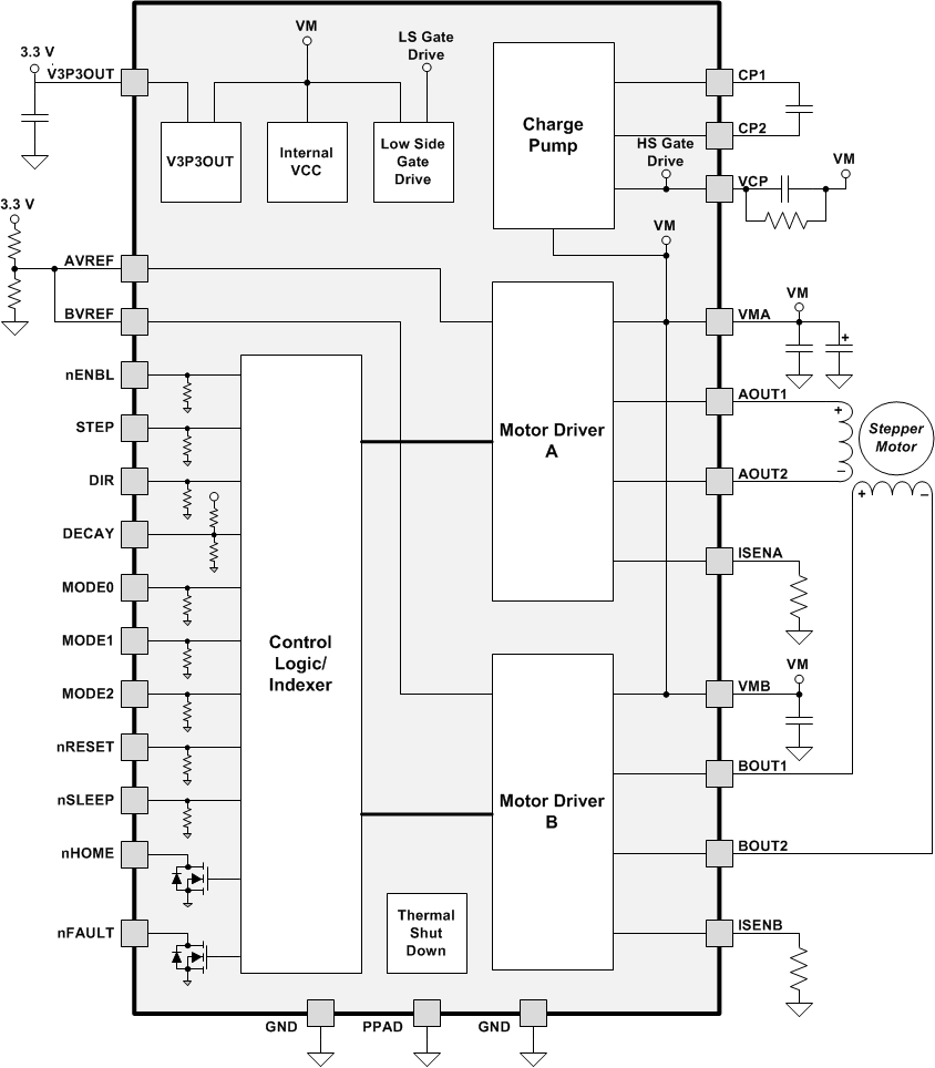
- 4 Simplified Schematic
- 5 Revision History
- 6 Terminal Configuration and Functions
- 7 Specifications
- 8 Detailed Description
- 9 Application and Implementation
- 10Power Supply Recommendations
- 11Layout
- 12Device and Documentation Support
- 13Mechanical, Packaging, and Orderable Information
Package Options
Mechanical Data (Package|Pins)
- PWP|28
Thermal pad, mechanical data (Package|Pins)
- PWP|28
Orderable Information
8 Detailed Description
8.1 Overview
The DRV8824-Q1 is an integrated motor driver solution for bipolar stepper motors. The device integrates two NMOS H-bridges, current sense and regulation circuitry, and a microstepping indexer. The DRV8824-Q1 can be powered with a supply voltage between 8.2 V and 45 V, and is capable of providing an output current up to 1.6 A full-scale or 1.1 A rms.
A simple STEP/DIR interface allows easy interfacing to the controller circuit. The internal indexer is able to execute high-accuracy microstepping without requiring the processor to control the current level.
The current regulation is highly configurable, with three decay modes of operation. Fast, slow, and mixed decay can be used.
A low-power sleep mode is included which allows the system to save power when not driving the motor.
8.2 Functional Block Diagram
8.3 Feature Description
8.3.1 PWM Motor Drivers
The DRV8824-Q1 contains two H-bridge motor drivers with current-control PWM circuitry. A block diagram of the motor control circuitry is shown in Figure 6.
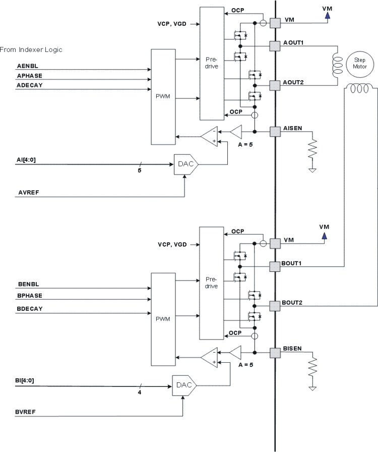 Figure 6. Motor Control Circuitry
Note that there are multiple VM motor power supply terminals. All VM terminals must be connected together to the motor supply voltage.
8.3.2 Current Regulation
The current through the motor windings is regulated by a fixed-frequency PWM current regulation, or current chopping. When an H-bridge is enabled, current rises through the winding at a rate dependent on the DC voltage and inductance of the winding. Once the current hits the current chopping threshold, the bridge disables the current until the beginning of the next PWM cycle.
In stepping motors, current regulation is used to vary the current in the two windings in a semi-sinusoidal fashion to provide smooth motion.
The PWM chopping current is set by a comparator which compares the voltage across a current sense resistor connected to the xISEN terminals, multiplied by a factor of 5, with a reference voltage. The reference voltage is input from the xVREF terminals.
The full-scale (100%) chopping current is calculated in Equation 1.
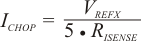
Example:
If a 0.5-Ω sense resistor is used and the VREFx terminal is 3.3 V, the full-scale (100%) chopping current will be 3.3 V / (5 x 0.5 Ω) = 1.32 A.
The reference voltage is scaled by an internal DAC that allows fractional stepping of a bipolar stepper motor, as described in the microstepping indexer section below.
8.3.3 Blanking Time
After the current is enabled in an H-bridge, the voltage on the xISEN terminal is ignored for a fixed period of time before enabling the current sense circuitry. This blanking time is fixed at 3.75 μs. Note that the blanking time also sets the minimum on time of the PWM.
8.3.4 Microstepping Indexer
Built-in indexer logic in the DRV8824-Q1 allows a number of different stepping configurations. The MODE0 - MODE2 terminals are used to configure the stepping format as shown in .
Table 1. Stepping Format
| MODE2 | MODE1 | MODE0 | STEP MODE |
|---|---|---|---|
| 0 | 0 | 0 | Full step (2-phase excitation) with 71% current |
| 0 | 0 | 1 | 1/2 step (1-2 phase excitation) |
| 0 | 1 | 0 | 1/4 step (W1-2 phase excitation) |
| 0 | 1 | 1 | 8 microsteps / step |
| 1 | 0 | 0 | 16 microsteps / step |
| 1 | 0 | 1 | 32 microsteps / step |
| 1 | 1 | 0 | 32 microsteps / step |
| 1 | 1 | 1 | 32 microsteps / step |
Table 2 shows the relative current and step directions for different settings of MODEx. At each rising edge of the STEP input, the indexer travels to the next state in the table. The direction is shown with the DIR terminal high; if the DIR terminal is low the sequence is reversed. Positive current is defined as xOUT1 = positive with respect to xOUT2.
Note that if the step mode is changed while stepping, the indexer will advance to the next valid state for the new MODEx setting at the rising edge of STEP.
The home state is 45°. This state is entered at power-up or application of nRESET. This is shown in Table 2 by the shaded cells. The logic inputs DIR, STEP, nRESET and MODEx have an internal pulldown resistors of
100 kΩ
Table 2. Relative Current and Step Directions
| 1/32 STEP | 1/16 STEP | 1/8 STEP | 1/4 STEP | 1/2 STEP | FULL STEP 70% |
WINDING CURRENT A |
WINDING CURRENT B |
ELECTRICAL ANGLE |
|---|---|---|---|---|---|---|---|---|
| 1 | 1 | 1 | 1 | 1 | 100% | 0% | 0 | |
| 2 | 100% | 5% | 3 | |||||
| 3 | 2 | 100% | 10% | 6 | ||||
| 4 | 99% | 15% | 8 | |||||
| 5 | 3 | 2 | 98% | 20% | 11 | |||
| 6 | 97% | 24% | 14 | |||||
| 7 | 4 | 96% | 29% | 17 | ||||
| 8 | 94% | 34% | 20 | |||||
| 9 | 5 | 3 | 2 | 92% | 38% | 23 | ||
| 10 | 90% | 43% | 25 | |||||
| 11 | 6 | 88% | 47% | 28 | ||||
| 12 | 86% | 51% | 31 | |||||
| 13 | 7 | 4 | 83% | 56% | 34 | |||
| 14 | 80% | 60% | 37 | |||||
| 15 | 8 | 77% | 63% | 39 | ||||
| 16 | 74% | 67% | 42 | |||||
| 17 | 9 | 5 | 3 | 2 | 1 | 71% | 71% | 45 |
| 18 | 67% | 74% | 48 | |||||
| 19 | 10 | 63% | 77% | 51 | ||||
| 20 | 60% | 80% | 53 | |||||
| 21 | 11 | 6 | 56% | 83% | 56 | |||
| 22 | 51% | 86% | 59 | |||||
| 23 | 12 | 47% | 88% | 62 | ||||
| 24 | 43% | 90% | 65 | |||||
| 25 | 13 | 7 | 4 | 38% | 92% | 68 | ||
| 26 | 34% | 94% | 70 | |||||
| 27 | 14 | 29% | 96% | 73 | ||||
| 28 | 24% | 97% | 76 | |||||
| 29 | 15 | 8 | 20% | 98% | 79 | |||
| 30 | 15% | 99% | 82 | |||||
| 31 | 16 | 10% | 100% | 84 | ||||
| 32 | 5% | 100% | 87 | |||||
| 33 | 17 | 9 | 5 | 3 | 0% | 100% | 90 | |
| 34 | –5% | 100% | 93 | |||||
| 35 | 18 | –10% | 100% | 96 | ||||
| 36 | –15% | 99% | 98 | |||||
| 37 | 19 | 10 | –20% | 98% | 101 | |||
| 38 | –24% | 97% | 104 | |||||
| 39 | 20 | –29% | 96% | 107 | ||||
| 40 | –34% | 94% | 110 | |||||
| 41 | 21 | 11 | 6 | –38% | 92% | 113 | ||
| 42 | –43% | 90% | 115 | |||||
| 43 | 22 | –47% | 88% | 118 | ||||
| 44 | –51% | 86% | 121 | |||||
| 45 | 23 | 12 | –56% | 83% | 124 | |||
| 46 | –60% | 80% | 127 | |||||
| 47 | 24 | –63% | 77% | 129 | ||||
| 48 | –67% | 74% | 132 | |||||
| 49 | 25 | 13 | 7 | 4 | 2 | –71% | 71% | 135 |
| 50 | –74% | 67% | 138 | |||||
| 51 | 26 | –77% | 63% | 141 | ||||
| 52 | –80% | 60% | 143 | |||||
| 53 | 27 | 14 | –83% | 56% | 146 | |||
| 54 | –86% | 51% | 149 | |||||
| 55 | 28 | –88% | 47% | 152 | ||||
| 56 | –90% | 43% | 155 | |||||
| 57 | 29 | 15 | 8 | –92% | 38% | 158 | ||
| 58 | –94% | 34% | 160 | |||||
| 59 | 30 | –96% | 29% | 163 | ||||
| 60 | –97% | 24% | 166 | |||||
| 61 | 31 | 16 | –98% | 20% | 169 | |||
| 62 | –99% | 15% | 172 | |||||
| 63 | 32 | –100% | 10% | 174 | ||||
| 64 | –100% | 5% | 177 | |||||
| 65 | 33 | 17 | 9 | 5 | –100% | 0% | 180 | |
| 66 | –100% | –5% | 183 | |||||
| 67 | 34 | –100% | –10% | 186 | ||||
| 68 | –99% | –15% | 188 | |||||
| 69 | 35 | 18 | –98% | –20% | 191 | |||
| 70 | –97% | –24% | 194 | |||||
| 71 | 36 | –96% | –29% | 197 | ||||
| 72 | –94% | –34% | 200 | |||||
| 73 | 37 | 19 | 10 | –92% | –38% | 203 | ||
| 74 | –90% | –43% | 205 | |||||
| 75 | 38 | –88% | –47% | 208 | ||||
| 76 | –86% | –51% | 211 | |||||
| 77 | 39 | 20 | –83% | –56% | 214 | |||
| 78 | –80% | –60% | 217 | |||||
| 79 | 40 | –77% | –63% | 219 | ||||
| 80 | –74% | –67% | 222 | |||||
| 81 | 41 | 21 | 11 | 6 | 3 | –71% | –71% | 225 |
| 82 | –67% | –74% | 228 | |||||
| 83 | 42 | –63% | –77% | 231 | ||||
| 84 | –60% | –80% | 233 | |||||
| 85 | 43 | 22 | –56% | –83% | 236 | |||
| 86 | –51% | –86% | 239 | |||||
| 87 | 44 | –47% | –88% | 242 | ||||
| 88 | –43% | –90% | 245 | |||||
| 89 | 45 | 23 | 12 | –38% | –92% | 248 | ||
| 90 | –34% | –94% | 250 | |||||
| 91 | 46 | –29% | –96% | 253 | ||||
| 92 | –24% | –97% | 256 | |||||
| 93 | 47 | 24 | –20% | –98% | 259 | |||
| 94 | –15% | –99% | 262 | |||||
| 95 | 48 | –10% | –100% | 264 | ||||
| 96 | –5% | –100% | 267 | |||||
| 97 | 49 | 25 | 13 | 7 | 0% | –100% | 270 | |
| 98 | 5% | –100% | 273 | |||||
| 99 | 50 | 10% | –100% | 276 | ||||
| 100 | 15% | –99% | 278 | |||||
| 101 | 51 | 26 | 20% | –98% | 281 | |||
| 102 | 24% | –97% | 284 | |||||
| 103 | 52 | 29% | –96% | 287 | ||||
| 104 | 34% | –94% | 290 | |||||
| 105 | 53 | 27 | 14 | 38% | –92% | 293 | ||
| 106 | 43% | –90% | 295 | |||||
| 107 | 54 | 47% | –88% | 298 | ||||
| 108 | 51% | –86% | 301 | |||||
| 109 | 55 | 28 | 56% | –83% | 304 | |||
| 110 | 60% | –80% | 307 | |||||
| 111 | 56 | 63% | –77% | 309 | ||||
| 112 | 67% | –74% | 312 | |||||
| 113 | 57 | 29 | 15 | 8 | 4 | 71% | –71% | 315 |
| 114 | 74% | –67% | 318 | |||||
| 115 | 58 | 77% | –63% | 321 | ||||
| 116 | 80% | –60% | 323 | |||||
| 117 | 59 | 30 | 83% | –56% | 326 | |||
| 118 | 86% | –51% | 329 | |||||
| 119 | 60 | 88% | –47% | 332 | ||||
| 120 | 90% | –43% | 335 | |||||
| 121 | 61 | 31 | 16 | 92% | –38% | 338 | ||
| 122 | 94% | –34% | 340 | |||||
| 123 | 62 | 96% | –29% | 343 | ||||
| 124 | 97% | –24% | 346 | |||||
| 125 | 63 | 32 | 98% | –20% | 349 | |||
| 126 | 99% | –15% | 352 | |||||
| 127 | 64 | 100% | –10% | 354 | ||||
| 128 | 100% | –5% | 357 |
8.3.5 nRESET, nENBLE and nSLEEP Operation
The nRESET terminal, when driven active low, resets internal logic, and resets the step table to the home position. It also disables the H-bridge drivers. The STEP input is ignored while nRESET is active.
The nENBL terminal is used to control the output drivers and enable/disable operation of the indexer. When nENBL is low, the output H-bridges are enabled, and rising edges on the STEP terminal are recognized. When nENBL is high, the H-bridges are disabled, the outputs are in a high-impedance state, and the STEP input is ignored.
Driving nSLEEP low will put the device into a low power sleep state. In this state, the H-bridges are disabled, the gate drive charge pump is stopped, the V3P3OUT regulator is disabled, and all internal clocks are stopped. In this state all inputs are ignored until nSLEEP returns inactive high. When returning from sleep mode, some time (approximately 1 ms) needs to pass before applying a STEP input, to allow the internal circuitry to stabilize.
The nRESET and nENABLE terminals have internal pulldown resistors of 100 kΩ. The nSLEEP terminal has an internal pulldown resistor of 1 MΩ.
8.3.6 Protection Circuits
The DRV8824-Q1 is fully protected against undervoltage, overcurrent and overtemperature events.
8.3.6.1 Overcurrent Protection (OCP)
An analog current limit circuit on each FET limits the current through the FET by removing the gate drive. If this analog current limit persists for longer than the OCP time, all FETs in the H-bridge will be disabled and the nFAULT terminal will be driven low. The device will remain disabled until either nRESET terminal is applied, or VM is removed and re-applied.
Overcurrent conditions on both high and low side devices; i.e., a short to ground, supply, or across the motor winding will all result in an overcurrent shutdown. Note that overcurrent protection does not use the current sense circuitry used for PWM current control, and is independent of the ISENSE resistor value or VREF voltage.
8.3.6.2 Thermal Shutdown (TSD)
If the die temperature exceeds safe limits, all FETs in the H-bridge will be disabled and the nFAULT terminal will be driven low. Once the die temperature has fallen to a safe level operation will automatically resume.
8.3.6.3 Undervoltage Lockout (UVLO)
If at any time the voltage on the VM terminals falls below the undervoltage lockout threshold voltage, all circuitry in the device will be disabled and internal logic will be reset. Operation will resume when VM rises above the UVLO threshold.
8.3.7 Thermal Information
8.3.7.1 Thermal Protection
The DRV8824-Q1 has thermal shutdown (TSD) as described above. If the die temperature exceeds approximately 150°C, the device will be disabled until the temperature drops to a safe level.
Any tendency of the device to enter TSD is an indication of either excessive power dissipation, insufficient heatsinking, or too high an ambient temperature.
8.3.7.2 Power Dissipation
Power dissipation in the DRV8824-Q1 is dominated by the power dissipated in the output FET resistance, or RDS(ON). Average power dissipation when running a stepper motor can be roughly estimated by Equation 2.

where PTOT is the total power dissipation, RDS(ON) is the resistance of each FET, and IOUT(RMS) is the RMS output current being applied to each winding. IOUT(RMS) is equal to the approximately 0.7x the full-scale output current setting. The factor of 4 comes from the fact that there are two motor windings, and at any instant two FETs are conducting winding current for each winding (one high-side and one low-side).
The maximum amount of power that can be dissipated in the device is dependent on ambient temperature and heatsinking.
Note that RDS(ON) increases with temperature, so as the device heats, the power dissipation increases. This must be taken into consideration when sizing the heatsink.
8.3.7.3 Heatsinking
The PowerPAD™ package uses an exposed pad to remove heat from the device. For proper operation, this pad must be thermally connected to copper on the PCB to dissipate heat. On a multi-layer PCB with a ground plane, this can be accomplished by adding a number of vias to connect the thermal pad to the ground plane. On PCBs without internal planes, copper area can be added on either side of the PCB to dissipate heat. If the copper area is on the opposite side of the PCB from the device, thermal vias are used to transfer the heat between top and bottom layers.
For details about how to design the PCB, refer to TI application report SLMA002, "PowerPAD™ Thermally Enhanced Package" and TI application brief SLMA004, "PowerPAD™ Made Easy", available at www.ti.com.
In general, the more copper area that can be provided, the more power can be dissipated. It can be seen that the heatsink effectiveness increases rapidly to about 20 cm2, then levels off somewhat for larger areas.
8.4 Device Functional Modes
8.4.1 Decay Mode
During PWM current chopping, the H-bridge is enabled to drive current through the motor winding until the PWM current chopping threshold is reached. This is shown in Figure 7 as case 1. The current flow direction shown indicates positive current flow.
Once the chopping current threshold is reached, the H-bridge can operate in two different states, fast decay or slow decay.
In fast decay mode, once the PWM chopping current level has been reached, the H-bridge reverses state to allow winding current to flow in a reverse direction. As the winding current approaches zero, the bridge is disabled to prevent any reverse current flow. Fast decay mode is shown in Figure 7 as case 2.
In slow decay mode, winding current is re-circulated by enabling both of the low-side FETs in the bridge. This is shown in Figure 7 as case 3.
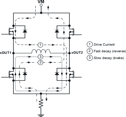 Figure 7. Decay Mode
The DRV8824-Q1 supports fast decay, slow decay and a mixed decay mode. Slow, fast, or mixed decay mode is selected by the state of the DECAY terminal - logic low selects slow decay, open selects mixed decay operation, and logic high sets fast decay mode. The DECAY terminal has both an internal pullup resistor of approximately 130 kΩ and an internal pulldown resistor of approximately 80 kΩ. This sets the mixed decay mode if the terminal is left open or undriven.
Mixed decay mode begins as fast decay, but at a fixed period of time (75% of the PWM cycle) switches to slow decay mode for the remainder of the fixed PWM period. This occurs only if the current through the winding is decreasing (per the indexer step table); if the current is increasing, then slow decay is used.