SLVSCH0 April 2014 DRV8824-Q1
PRODUCTION DATA.
- 1 Features
- 2 Applications
- 3 Description
- 4 Simplified Schematic
- 5 Revision History
- 6 Terminal Configuration and Functions
- 7 Specifications
- 8 Detailed Description
- 9 Application and Implementation
- 10Power Supply Recommendations
- 11Layout
- 12Device and Documentation Support
- 13Mechanical, Packaging, and Orderable Information
Package Options
Mechanical Data (Package|Pins)
- PWP|28
Thermal pad, mechanical data (Package|Pins)
- PWP|28
Orderable Information
6 Terminal Configuration and Functions
PWP Package
(Top View)
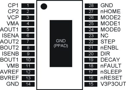
Terminal Functions
| NAME | TERMINAL | I/O | DESCRIPTION | EXTERNAL COMPONENTS OR CONNECTIONS |
|---|---|---|---|---|
| POWER AND GROUND | ||||
| GND | 14, 28 | - | Device ground | |
| VMA | 4 | - | Bridge A power supply | Connect to motor supply (8.2 V - 45 V). Both terminals must be connected to same supply. |
| VMB | 11 | - | Bridge B power supply | |
| V3P3OUT | 15 | O | 3.3-V regulator output | Bypass to GND with a 0.47-μF 6.3-V ceramic capacitor. Can be used to supply VREF. |
| CP1 | 1 | IO | Charge pump flying capacitor | Connect a 0.01-μF 50-V capacitor between CP1 and CP2. |
| CP2 | 2 | IO | Charge pump flying capacitor | |
| VCP | 3 | IO | High-side gate drive voltage | Connect a 0.1-μF 16-V ceramic capacitor and a 1-MΩ resistor to VM. |
| CONTROL | ||||
| nENBL | 21 | I | Enable input | Logic high to disable device outputs and indexer operation, logic low to enable. Internal pulldown. |
| nSLEEP | 17 | I | Sleep mode input | Logic high to enable device, logic low to enter low-power sleep mode. Internal pulldown. |
| STEP | 22 | I | Step input | Rising edge causes the indexer to move one step. Internal pulldown. |
| DIR | 20 | I | Direction input | Level sets the direction of stepping. Internal pulldown. |
| MODE0 | 24 | I | Microstep mode 0 | MODE0 - MODE2 set the step mode - full, 1/2, 1/4, 1/8/ 1/16, or 1/32 step. Internal pulldown. |
| MODE1 | 25 | I | Microstep mode 1 | |
| MODE2 | 26 | I | Microstep mode 2 | |
| DECAY | 19 | I | Decay mode | Low = slow decay, open = mixed decay, high = fast decay. Internal pulldown and pullup. |
| nRESET | 16 | I | Reset input | Active-low reset input initializes the indexer logic and disables the H-bridge outputs. Internal pulldown. |
| AVREF | 12 | I | Bridge A current set reference input | Reference voltage for winding current set. Normally AVREF and BVREF are connected to the same voltage. Can be connected to V3P3OUT. A 0.01-µF bypass capacitor to GND is recommended. |
| BVREF | 13 | I | Bridge B current set reference input | |
| NC | 23 | No connect | Leave this terminal unconnected. | |
| STATUS | ||||
| nHOME | 27 | OD | Home position | Logic low when at home state of step table |
| nFAULT | 18 | OD | Fault | Logic low when in fault condition (overtemp, overcurrent) |
| OUTPUT | ||||
| ISENA | 6 | IO | Bridge A ground / Isense | Connect to current sense resistor for bridge A. |
| ISENB | 9 | IO | Bridge B ground / Isense | Connect to current sense resistor for bridge B. |
| AOUT1 | 5 | O | Bridge A output 1 | Connect to bipolar stepper motor winding A. Positive current is AOUT1 → AOUT2 |
| AOUT2 | 7 | O | Bridge A output 2 | |
| BOUT1 | 10 | O | Bridge B output 1 | Connect to bipolar stepper motor winding B. Positive current is BOUT1 → BOUT2 |
| BOUT2 | 8 | O | Bridge B output 2 | |