SLVSAB2G May 2010 – December 2015 DRV8830
PRODUCTION DATA.
- 1 Features
- 2 Applications
- 3 Description
- 4 Revision History
- 5 Pin Configuration and Functions
- 6 Specifications
- 7 Detailed Description
- 8 Application and Implementation
- 9 Power Supply Recommendations
- 10Layout
- 11Device and Documentation Support
- 12Mechanical, Packaging, and Orderable Information
Package Options
Mechanical Data (Package|Pins)
Thermal pad, mechanical data (Package|Pins)
Orderable Information
8 Application and Implementation
NOTE
Information in the following applications sections is not part of the TI component specification, and TI does not warrant its accuracy or completeness. TI’s customers are responsible for determining suitability of components for their purposes. Customers should validate and test their design implementation to confirm system functionality.
8.1 Application Information
The DRV8830 is used in brushed DC applications to provide a constant motor speed over varying voltages. The following design procedure can be used to configure the DRV8830 for a system with a VCC variance of 4 to 6 V.
8.2 Typical Application
Figure 11 is a common application of the DRV8830.
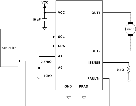 Figure 11. Motor Control Circuitry
8.2.1 Design Requirements
Table 9 lists the design parameters of the DRV8830.
Table 9. Design Parameters
| DESIGN PARAMETER | REFERENCE | EXAMPLE VALUE | |||
|---|---|---|---|---|---|
| Motor voltage | VCC | 5 V | |||
| Motor RMS current | IRMS | 0.3 A | |||
| Motor start-up | ISTART | 1.3 A | |||
| Motor current trip point | ILIMIT | 0.9 A | |||
8.2.2 Detailed Design Procedure
8.2.2.1 Motor Voltage
The motor voltage to use will depend on the ratings of the motor selected and the desired RPM. A higher voltage spins a brushed DC motor faster with the same PWM duty cycle applied to the power FETs. A higher voltage also increases the rate of current change through the inductive motor windings.
For the DRV8830, TI recommends to set a motor voltage at the lowest system VCC. This will maintain a constant RPM across varying VCC conditions.
For example if the VCC voltage can vary from 4.5V to 5.5V, setting the VSET voltage to 1.125 V will compensate for power supply variation. The DRV8830 will set the motor voltage at 4.5 V, even if VCC is 5.5 V.
8.2.2.2 Motor Current Trip Point
When the voltage on pin ISENSE exceeds VILIM (0.2 V), overcurrent is detected. The RSENSE resistor should be sized to set the desired ILIMIT level.
To set IILIMIT to 0.5 A, RISENSE = 0.2 V / 0.9 A = 0.22 Ω.
To prevent false trips, ILIMIT must be higher than regular operating current. Motor current during start-up is typically much higher than steady-state spinning, because the initial load torque is higher, and the absence of back-EMF causes a higher voltage and extra current across the motor windings.
It can be beneficial to limit start-up current by using series inductors on the DRV8830 output, as that allows ILIMIT to be lower, and it may decrease the system’s required bulk capacitance. Start-up current can also be limited by ramping the forward drive duty cycle.
8.2.2.3 Sense Resistor Selection
For optimal performance, it is important for the sense resistor to be:
- Surface-mount
- Low inductance
- Rated for high enough power
- Placed closely to the motor driver
The power dissipated by the sense resistor equals IRMS2 × R. For example, if peak motor current is 1 A, RMS motor current is 0.7 A, and a 0.4-Ω sense resistor is used, the resistor will dissipate 0.7 A2 × 0.4 Ω = 0.2 W. The power quickly increases with higher current levels.
Resistors typically have a rated power within some ambient temperature range, along with a de-rated power curve for high ambient temperatures. When a PCB is shared with other components generating heat, margin should be added. It is always best to measure the actual sense resistor temperature in a final system, along with the power MOSFETs, as those are often the hottest components.
Because power resistors are larger and more expensive than standard resistors, it is common practice to use multiple standard resistors in parallel, between the sense node and ground. This distributes the current and heat dissipation.
8.2.2.4 Low Power Operation
Under normal operation, using sleep mode to minimize supply current should be sufficient.
If desired, power can be removed to the DRV8830 to further decrease supply current. TI recommends to remove power to the FAULTn pullup resistor when removing power to the DRV8830. Removing power from the FAULTn pullup resistor will eliminate a current path from the FAULTn pin through an ESD protection diode to VCC. TI recommends to set both IN1 and IN2 as a logic low when power is removed.
An undervoltage event may cause the address to be re-evaluated. If this occurs, the I2C interface may stop working until power is cycled.
8.2.3 Application Curves
The following scope captures show how the output duty cycle changes to as VCC increases. This allows the motor to spin at a constant speed as VCC changes. At VCC = 3.9 V, the output duty cycle is 100% on. As the VCC voltage increases to greater than 4 V, the output duty cycle begins to decrease. The output duty cycle is shown at VCC = 4.5 V, VCC = 5 V and VCC = 5.5 V.
- Channel 1 – OUT1: IN1 – Logic Low
- Channel 2 – OUT2: IN2 – Logic High
- Channel 4 – Motor current: VSET – 1 V
- Motor used: NMB Technologies Corporation, PPN7PA12C1
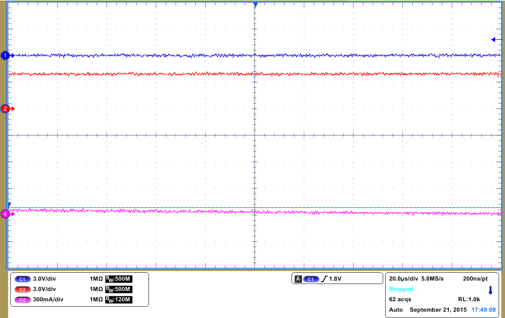 Figure 12. Output Pulse Width Modulating at VCC = 3.9 V
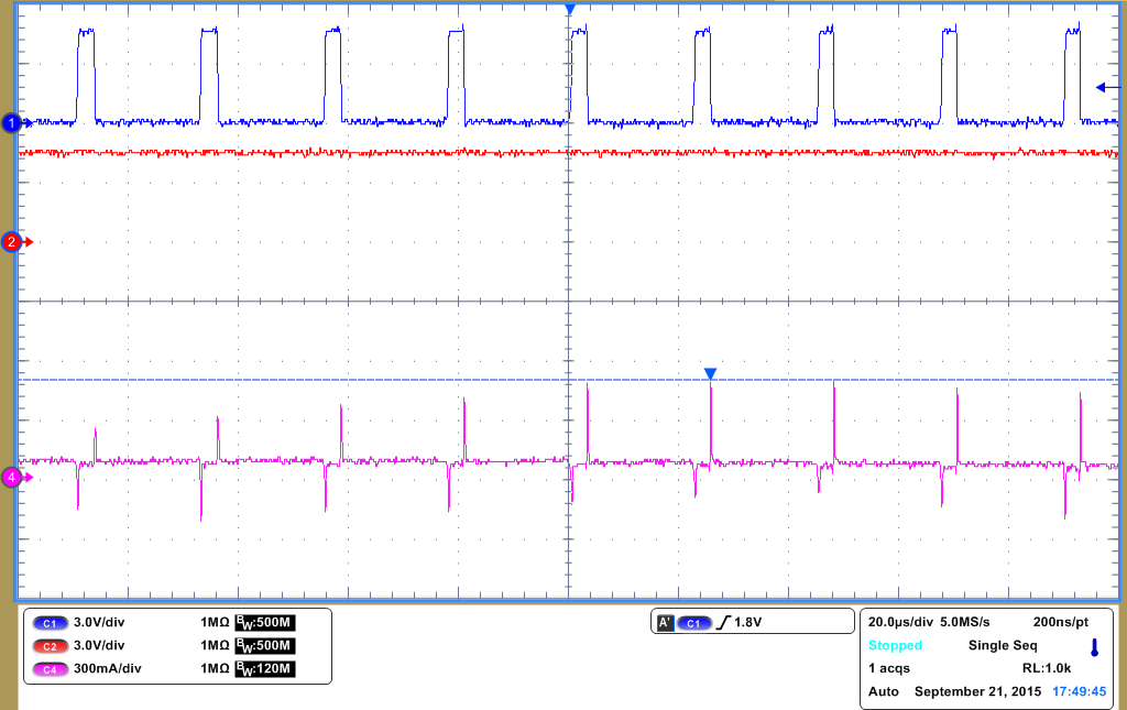 Figure 14. Output Pulse Width Modulating at VCC = 4.5 V
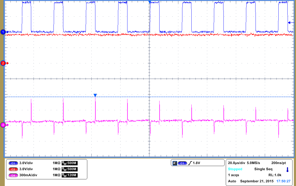 Figure 16. Output Pulse Width Modulating at VCC = 5.5 V
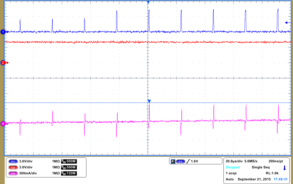 Figure 13. Output Pulse Width Modulating at VCC = 4 V
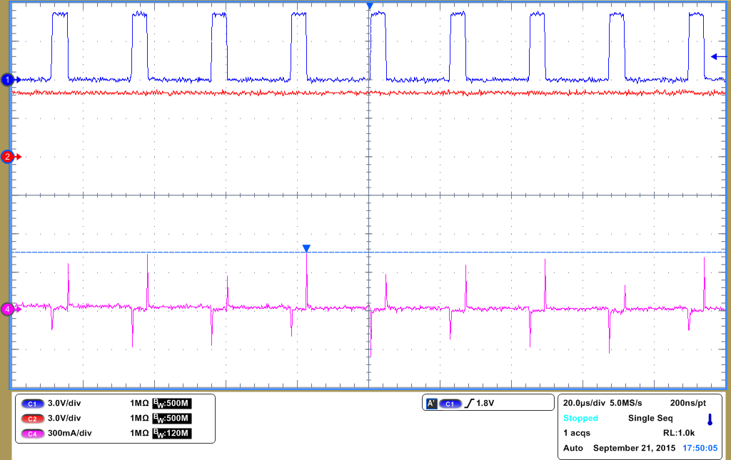 Figure 15. Output Pulse Width Modulating at VCC = 5 V