SLVSBW9C April   2013  – December 2015 DRV8832-Q1

PRODUCTION DATA.  

  1. Features
  2. Applications
  3. Description
    1.     Device Images
      1.      Simplified Schematic
  4. Revision History
  5. Pin Configuration and Functions
    1.     Pin Functions
  6. Specifications
    1. 6.1 Absolute Maximum Ratings
    2. 6.2 ESD Ratings
    3. 6.3 Recommended Operating Conditions
    4. 6.4 Thermal Information
    5. 6.5 Electrical Characteristics
    6. 6.6 Typical Characteristics
  7. Detailed Description
    1. 7.1 Overview
    2. 7.2 Functional Block Diagram
    3. 7.3 Feature Description
      1. 7.3.1 PWM Motor Driver
      2. 7.3.2 Bridge Control
      3. 7.3.3 Voltage Regulation
      4. 7.3.4 Reference Output
      5. 7.3.5 Current Limit
      6. 7.3.6 Protection Circuits
        1. 7.3.6.1 Overcurrent Protection (OCP)
        2. 7.3.6.2 Thermal Shutdown (TSD)
        3. 7.3.6.3 Undervoltage Lockout (UVLO)
    4. 7.4 Device Functional Modes
  8. Application and Implementation
    1. 8.1 Application Information
    2. 8.2 Typical Application
      1. 8.2.1 Design Requirements
      2. 8.2.2 Detailed Design Procedure
        1. 8.2.2.1 Motor Voltage
        2. 8.2.2.2 Motor Current Trip Point
        3. 8.2.2.3 Sense Resistor Selection
        4. 8.2.2.4 Low Power Operation
      3. 8.2.3 Application Curves
  9. Power Supply Recommendations
    1. 9.1 Power Supervisor
    2. 9.2 Bulk Capacitance
  10. 10Layout
    1. 10.1 Layout Guidelines
    2. 10.2 Layout Example
    3. 10.3 Thermal Considerations
      1. 10.3.1 Power Dissipation
      2. 10.3.2 Heatsinking
  11. 11Device and Documentation Support
    1. 11.1 Documentation Support
      1. 11.1.1 Related Documentation
    2. 11.2 Community Resources
    3. 11.3 Trademarks
    4. 11.4 Electrostatic Discharge Caution
    5. 11.5 Glossary
  12. 12Mechanical, Packaging, and Orderable Information

Package Options

Refer to the PDF data sheet for device specific package drawings

Mechanical Data (Package|Pins)
  • DGQ|10
Thermal pad, mechanical data (Package|Pins)
Orderable Information

Typical Characteristics

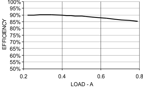
DRV8832-Q1 eff_vs_iload_lvsab2.gif
Figure 1. Efficiency vs Load Current (VIN = 5 V, VOUT = 3 V)
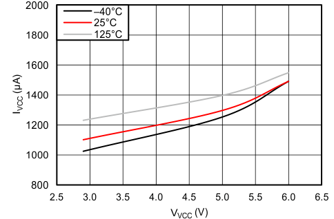
DRV8832-Q1 C001_SLVSBW9.gif
Figure 3. IVCC vs VVCC
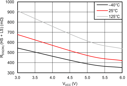
DRV8832-Q1 C003_SLVSBW9.gif
Figure 5. RDS(on) HS + LS vs VVCC
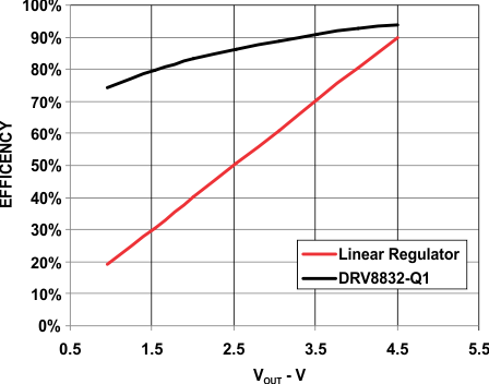
DRV8832-Q1 eff_vs_vout_lvsbw9.gif
Figure 2. Efficiency vs Output Voltage (VIN = 5 V,
IOUT = 500 mA)
DRV8832-Q1 C002_SLVSBW9.gif
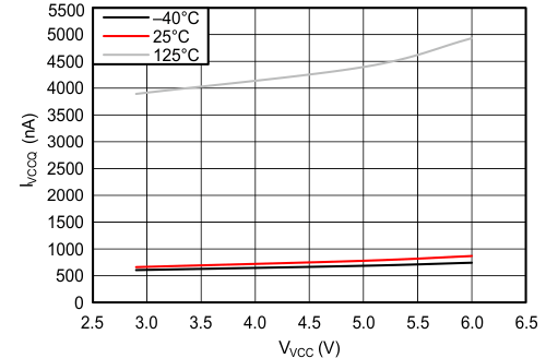
Figure 4. IVCCQ vs VVCC
DRV8832-Q1 C004_SLVSBW9.gif
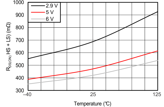
Figure 6. RDS(on) HS + LS vs Temperature