SLVSBW9C April 2013 – December 2015 DRV8832-Q1
PRODUCTION DATA.
- 1 Features
- 2 Applications
- 3 Description
- 4 Revision History
- 5 Pin Configuration and Functions
- 6 Specifications
- 7 Detailed Description
- 8 Application and Implementation
- 9 Power Supply Recommendations
- 10Layout
- 11Device and Documentation Support
- 12Mechanical, Packaging, and Orderable Information
Package Options
Refer to the PDF data sheet for device specific package drawings
Mechanical Data (Package|Pins)
- DGQ|10
Thermal pad, mechanical data (Package|Pins)
- DGQ|10
Orderable Information
7.3.3 Voltage Regulation
The DRV8832-Q1 provides the ability to regulate the voltage applied to the motor winding. This feature allows constant motor speed to be maintained even when operating from a varying supply voltage such as a discharging battery.
The DRV8832-Q1 uses a pulse-width modulation (PWM) technique instead of a linear circuit to minimize current consumption and maximize battery life.
The circuit monitors the voltage difference between the output pins and integrates it, to get an average DC voltage value. This voltage is divided by 4 and compared to the VSET pin voltage. If the averaged output voltage (divided by 4) is lower than VSET, the duty cycle of the PWM output is increased; if the averaged output voltage (divided by 4) is higher than VSET, the duty cycle is decreased.
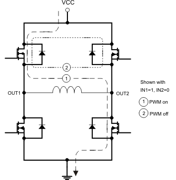
During PWM regulation, the H-bridge is enabled to drive current through the motor winding during the PWM on time. This is shown in Figure 8 as case 1. The current flow direction shown indicates the state when IN1 is high and IN2 is low.
Note that if the programmed output voltage is greater than the supply voltage, the device will operate at 100% duty cycle and the voltage regulation feature will be disabled. In this mode the device behaves as a conventional H-bridge driver.
During the PWM off time, winding current is re-circulated by enabling both of the high-side FETs in the bridge. This is shown as case 2 in Figure 8.
 Figure 8. Voltage Regulation